PCB design steps/difficulities/softwares
FR-4 PCB Manufacturing process-PCB design steps
PCB design steps1. Determine Requirements and Functions:
- At this initial and crucial stage, the design team needs to conduct comprehensive and in-depth research. Engage in multiple rounds of communication with product managers, end-users, and other relevant stakeholders to accurately understand the expected usage, performance standards, and market positioning of the product. Not only is it necessary to clearly understand the various types of signals that the equipment needs to handle, such as analog, digital, high-frequency, or low-frequency, but also to grasp the characteristics of its operating environment, including conditions such as temperature, humidity, and electromagnetic interference. At the same time, conduct a detailed analysis of the stability, efficiency, and power requirements of the power supply under different working modes. In addition, it is necessary to consider the interface specifications of the equipment with external systems, such as communication protocols, data transmission rates, and compatibility requirements. Through this series of efforts, a solid and clear functional framework is established for the subsequent design work.
PCB design steps2. Circuit Schematic Design:
- With the aid of advanced Electronic Design Automation (EDA) software, designers are like highly skilled architects, beginning to meticulously construct the blueprint of the circuit. They select suitable electronic components from the extensive component library. Each component is like a unique component in a building, with specific functions and electrical characteristics. These components include but are not limited to resistors, capacitors, inductors, diodes, transistors, integrated circuit chips, etc. Relying on profound circuit theory knowledge and practical experience, designers layout and connect these components in a logically clear and functionally explicit manner. The lines drawn represent the paths of current and the flow directions of signals, forming a complex yet orderly circuit schematic. During this process, it is necessary to precisely set the parameter values of each component to ensure that the circuit can theoretically achieve the expected functions. At the same time, the interaction and potential interference between components need to be fully considered to lay a solid theoretical foundation for the subsequent actual production.

PCB design steps3. Component Selection:
- Based on the drawn circuit schematic, it enters the crucial component selection stage. This requires designers to have extensive and in-depth knowledge of numerous electronic components in the market. They need to comprehensively consider multiple factors, such as the performance specifications of the components, including but not limited to the operating frequency range, accuracy, voltage and current withstand capabilities, to ensure that the selected components can perfectly match the functional requirements of the circuit. At the same time, the cost factor cannot be ignored. Under the premise of meeting performance requirements, components with high cost performance should be selected as much as possible to control the overall cost budget of the product. In addition, the supply stability and substitutability of components are also important considerations to avoid affecting the entire production progress due to the shortage of individual components. For components in some critical positions, attention should also be paid to their reliability and durability to ensure the stability and safety of the product during long-term use. Through careful weighing of these factors, the most suitable models and specifications are selected from numerous component options, laying a solid material foundation for achieving high-quality PCB design.
PCB design steps 4. Plan PCB Layout:
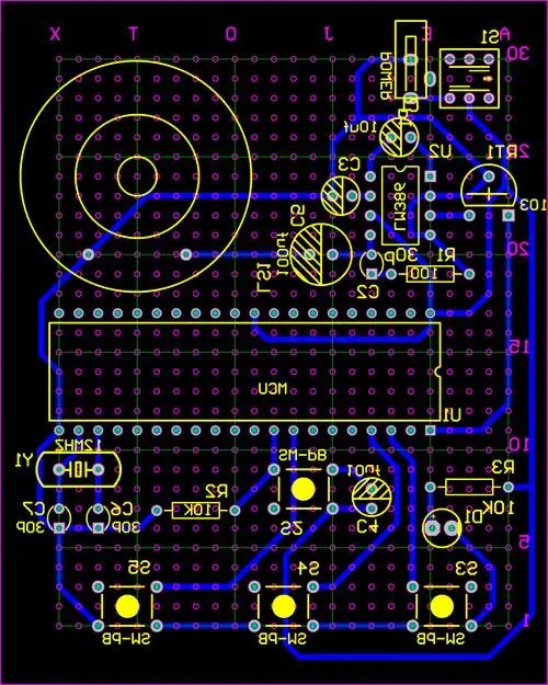
- At this stage, designers need to transform the abstract circuit schematic into an actual physical layout. They must first fully consider the physical size, shape, and installation methods of each electronic component to find a suitable "habitat" for them on the PCB board. At the same time, it is necessary to estimate the heat generated by the components during operation and arrange a reasonable heat dissipation space to ensure good thermal management and prevent local overheating from affecting circuit performance and component lifespan. For high-speed signal lines, the layout should follow the principle of signal flow direction to reduce signal reflection and crosstalk. In addition, attention should be paid to the partitioning of analog circuits and digital circuits to avoid mutual interference. The layout of the power supply lines is also crucial, ensuring a stable power supply and a low-impedance path to reduce power noise impact on the entire circuit. By comprehensively considering these factors, a preliminary layout plan that not only meets the circuit functional requirements but is also convenient for subsequent wiring and manufacturing is formulated.
PCB design steps 5. Wiring:
- The wiring stage is like building a transportation network in this microscopic city of the PCB. Designers use the powerful functions of EDA software to carefully connect the pins of each component. They need to strictly follow electrical rules and manufacturing requirements, and carefully set the length, width, and spacing of the lines. For high-speed signal lines, impedance control wiring technology is adopted to ensure signal integrity and transmission quality. For power supply lines and ground lines, a low-impedance path should be provided to stabilize the power supply and reduce electromagnetic interference. During the wiring process, it is also necessary to skillfully avoid possible interference sources, just like carefully planning urban roads to avoid traffic congestion and accidents. At the same time, it is necessary to make full use of the multi-layer structure of the PCB and reasonably layer the wiring to increase wiring density and reduce crossovers. The direction and layout of each line are carefully considered, aiming to build an efficient, stable, and interference-free circuit connection network.
PCB design steps 6. Design Rule Check (DRC):
- When the wiring work is completed, the rigorous design rule check is like conducting a comprehensive planning review of the elaborately constructed city. The EDA software will automatically scan and verify the PCB design based on a series of pre-set strict rules. These rules cover many aspects, from the minimum spacing of lines, the size and number of vias, to the correctness of inter-layer connections, and the rationality of component layout. The software will meticulously check for fatal errors such as short circuits and open circuits, as well as potential problems that may affect circuit performance and manufacturing feasibility, such as insufficient spacing and illegal routing. Once violations are found, warnings will be issued promptly, providing designers with accurate positioning and detailed error reports so that they can quickly make corrections and optimizations to ensure that the design meets the requirements of the manufacturing process and electrical performance standards.
PCB design steps 7. Signal Integrity and Power Integrity Analysis:
- For complex and high-speed PCB designs, signal integrity and power integrity analysis are particularly critical. This process is like a "health check" for the circuit. Through professional simulation software and analysis tools, various characteristics of the signal during transmission are evaluated, including but not limited to signal reflection, attenuation, crosstalk, and timing deviation. For the power supply system, its supply stability, voltage fluctuation, current distribution, and noise level are analyzed. Based on the analysis results, designers can identify potential signal distortion and power instability areas, and then take targeted measures, such as adding matching resistors, termination capacitors, decoupling capacitors, optimizing line layout and power layer segmentation to ensure accurate signal transmission and reliable power supply, thereby ensuring the high performance and stability of the entire circuit system.
PCB design steps 8. Optimize Design:
- Based on the previous analysis results, enter the optimization design stage, which is like carrying out refined transformation and improvement of the initially built city. Designers make targeted adjustments to the PCB layout and wiring based on the problems revealed by the signal integrity and power integrity analyses. It may be necessary to re-plan the positions of components to improve the signal path and reduce interference; adjust the routing and inter-layer distribution to optimize impedance matching and reduce crosstalk; add or adjust components such as capacitors and resistors to enhance decoupling and filtering effects. In addition, the thermal management will be re-evaluated and optimized to ensure there are sufficient heat dissipation channels around high-power components. Through continuous iteration and improvement, the PCB design achieves the best balance among performance, reliability, and cost.
PCB design steps 9. Generate Manufacturing Files:
- When the design is repeatedly optimized to the ideal state, the next step is to generate detailed manufacturing files, which is a key step in transforming the design into an actual product. These files include the definition of the PCB's layer stack structure, precisely describing the material, thickness, and function of each layer; drilling files, detailing the positions, diameters, and types of holes; silkscreen files, used to identify the positions, numbers, and other relevant information of components; solder mask files, determining the coverage area of the solder resist, etc. In addition, it also includes some test files and assembly guidelines, providing clear and accurate guidance for manufacturers to ensure that they can accurately produce high-quality PCB products in accordance with the design requirements, thereby perfectly realizing the design concept.
What are the difficulties in PCB design?
PCB design faces many difficulties. Here are some common aspects:
1. PCB design Signal integrity: As the operating frequency of circuits increases, ensuring that signals are not distorted, reflected, or subject to crosstalk during transmission on the PCB becomes extremely challenging. The wiring of high-speed signals requires precise control of the impedance matching, length, and spacing of the lines.
2. PCB design Power integrity: Providing a stable and low-noise power supply for complex circuits is difficult. It is necessary to rationally plan the layout of power planes and decoupling capacitors to reduce the influence of power fluctuations and noise on circuit performance.
3. Electromagnetic compatibility (EMC): PCB design must meet electromagnetic compatibility standards, prevent the generation of electromagnetic interference and radiation to the outside world, and also have the ability to resist external electromagnetic interference.
4. Wiring density: Achieving high-density wiring in a limited space, especially when there are numerous components with dense pins, significantly increases the wiring difficulty. Ingenious layout and wiring strategies are required.
5. Thermal management: For PCB design high-power circuits, effective heat dissipation to prevent component overheating is a key issue. It is necessary to reasonably arrange the component positions, design heat dissipation channels, and select suitable heat dissipation materials.
6. Multilayer board design: Multilayer PCBs increase the complexity of the design. The interlayer connections and signal cross-layer transmission need to be carefully planned to ensure performance and reliability.
7. Manufacturability and cost: While meeting the design requirements, it is necessary to consider the manufacturing process limitations and cost factors of the PCB to avoid pcb designs that are too complex, resulting in high manufacturing costs or difficult production.
8. Component layout: Reasonably arranging the positions of various components requires considering the signal flow direction, electromagnetic compatibility, heat dissipation, and other factors, while also facilitating subsequent assembly and maintenance.
9. Simulation and verification: Accurately performing circuit performance simulation and verification to predict and solve potential problems requires professional simulation tools and knowledge.
10.PCB Design change management: During the design process, due to various reasons, multiple design changes may be required. Effectively managing these changes to avoid errors and confusion is a difficulty.
Different application scenarios and design requirements may lead to different focuses and difficulties. PCB designers need to comprehensively consider these factors to achieve high-quality PCB designs.
How to design and optimize high-speed PCB design routing?
The design and optimization of high-speed PCB routing can follow the following steps and strategies:
1. Signal integrity analysis
- Before routing, use professional simulation software to conduct signal integrity analysis of high-speed signals to predict possible reflection, crosstalk, and timing issues.
2. Control trace impedance
- PCB Design the width of the traces, the distance from the reference plane, and other parameters strictly in accordance with the characteristic impedance requirements of the selected transmission line type (such as microstrip line, stripline) to ensure good impedance matching of the signal during transmission.
3. Reduce trace length
- Shorten the trace length of high-speed signals as much as possible to reduce signal transmission delay and attenuation.
4. Reasonable layer stack PCB design
- Plan the layer stack structure of the PCB design, allocate dedicated signal layers for high-speed signals, and ensure that the adjacent reference planes are complete and close to provide a good return path.
5. Avoid right-angle traces
- Use 45-degree angles or arc-shaped traces to reduce signal reflection and radiation.
6. PCB design grouping and routing rules
- Group related high-speed signals and route them according to the same routing rules, such as equal length and equal spacing.
7. PCB design Isolation and shielding
- For sensitive high-speed signals, adopt isolation measures, such as adding ground isolation or using shielding layers to reduce external interference.
8. Optimize vias
- Control the size and number of vias to minimize the impedance discontinuity and signal reflection caused by vias.
9. Power and ground plane processing
- Design low-impedance power and ground planes to provide a stable reference potential and good decoupling for the signals.
10. Post-simulation verification
- After completing the routing, conduct signal integrity simulation verification again and make necessary adjustments and optimizations based on the results.
11. Follow design specifications
- Refer to relevant industry standards and design specifications, such as IPC specifications, to ensure the reliability and manufacturability of the design.
Through the comprehensive application of the above methods, high-speed PCB routing can be effectively designed and optimized to improve the performance and stability of the circuit.
Share some commonly used PCB design software.
The following are some commonly used PCB design software:
1. Altium Designer: It is powerful and provides comprehensive design tools and libraries, suitable for complex multi-layer PCB designs.
2. Cadence Allegro: It performs well in high-speed PCB design and is often used in the design of high-end electronic products.
3. Mentor Graphics PADS: It is easy to learn and use, and is suitable for small and medium-sized PCB design projects.
4. KiCad: An open-source and free PCB design software with continuously evolving functions and active community support.
5. Eagle: It offers multiple versions, including free and professional versions, suitable for users with different needs.
These PCB design software have their own characteristics. You can choose the suitable PCB design software according to your own needs and usage habits.


