What is the meaning of the "false eight" in the PCB stack?
We are in the PCB design is required to choose the stacking scheme of our board, a good stacking scheme can make our signal quality better, the board performance will be more stable, etc., we may have more or less contact with multi-layer board, that is, two layers up the board, then we do six-layer board when you have heard of the "false eight layers "What do you mean by "fake eight layers"? Is he a six-ply or an eight-ply? We need to understand the following two points of knowledge before we can figure this out.01, PCB lamination knowledge
Our PCB board is usually a core board, copper foil, semi-cured sheet (also known as PP sheet) and the composition of the solder resist oil.
Core board: composed of copper foil, solid resin material and glass fiber, the basic material for the production of PCBs, with a certain degree of hardness and thickness, and the two surface layers have copper foil.
Prepreg sheet (PP sheet): mainly composed of resin and reinforcing materials, reinforcing materials are divided into glass fiber cloth, paper-based, composite materials and other types, and the production of multilayer printed circuit board used in the semi-curing sheet (bonding sheet) is mostly glass fiber cloth to do the reinforcing material.
02, PCB impedance basics
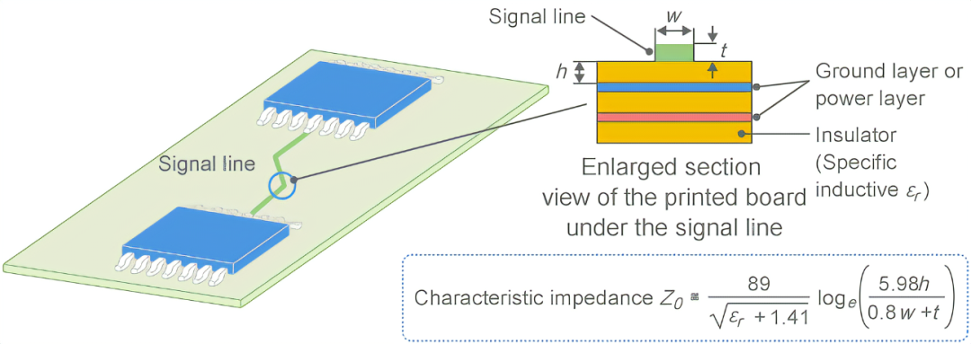
After we briefly understand the composition of our board, the following also need to understand a point of knowledge, that is, "impedance". With the rapid increase in signal transmission speed and the widespread use of high-frequency circuits, printed circuit boards also put forward higher requirements. Printed circuit boards must provide circuit performance that enables signals to be transmitted without reflections, signal integrity, reduced transmission losses and impedance matching, so that complete, reliable, accurate, interference-free and noise-free signals can be transmitted. Impedance matching is very important in high frequency design, impedance matching or not is related to the quality of the signal. The main purpose of impedance matching is to ensure that all microwave signals at high frequencies on the transmission line reach the load point and that no signals are reflected back to the source.
Usually the main factors affecting our impedance are the plate, dielectric constant, copper thickness, solder resist oil, line width, etc. If it is a differential line then the distance between the differential lines will also affect the impedance. General media thickness, differential line spacing and impedance is proportional to the relationship between the copper thickness, line width and impedance is inversely proportional to the relationship, general solder resist oil brush up will also reduce our impedance value.
After we know this knowledge, we can enter the subject, what is "false eight layers": the above figure shows a 1.6.1.2.2.2.
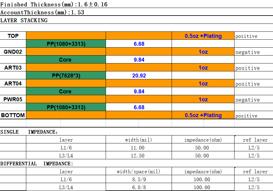
The above figure shows a 1.6mm board thickness six-layer board stack, he has two internal core board, a two-layer and five or six layers of pp sheet thickness of 6.68mil, core thickness is 9.84mil, core board and core board between the three pp sheet so the thickness reached 20.92mil, we use this stack design PCB, if we have a lot of impedance line above the board at this time We will find after calculation that the bottom of the table needs to control the 50om single-ended case line width is 11mil, 100om differential its line width line spacing of 8.5mil/9mil, while the inner layer of 50om single-ended line width reached 12.50mil, differential line width line spacing of 6.8mil/8mil.
This line width size undoubtedly increases the difficulty of our design, and may not even be designed, so we can change the method of stacking to achieve a lower line width and meet the impedance requirements, from the above impedance knowledge we understand that the media thickness and impedance value is proportional to the relationship, so if we want to reduce the line width of the surface layer can be reduced by reducing the number of pp sheet between the surface layer and the second layer and Choose a thinner type of pp sheet to reduce the thickness of the medium, at this time the thickness of the medium is reduced, the impedance value will also be small, then the line width can be reduced to achieve our target impedance value, due to the symmetry of the stacked layer so the bottom layer is also reduced by this method of line width.
The third layer is a reference to the second and fifth layer, where the third layer is closer to the second GND plane, the fifth layer is farther away from the third layer, we mainly refer to the second GND plane, a little more influenced by the second layer, so we can change the type of core board to reduce the value of the core, the media thickness is reduced, the third layer of the same line width of the impedance value is smaller, then we want to achieve the target impedance value is also the same to reduce the line width on it, so the inner layer also achieved to reduce the line width and meet the requirements of impedance, the fourth layer is also the same, but this time we will find that the first two layers and five or six layers between the pp sheet have become thinner, the core board has also become thinner, this time to achieve the target board thickness can only increase the thickness between the core board and the core board, we can increase the number of pp sheet to achieve the thickening of the However, we cannot keep increasing the number of pp sheets, generally only a maximum of three pp sheets can be used, the number of too many cases in the board pressed together when the board will appear the risk of slippage, we have introduced above the composition of the core board and pp sheets, both contain resin and glass fibre, but the core board has a copper foil on each side, we can add another piece between the core board and the core board We can add a "core board" between the core board and the core board to meet our board thickness requirements, but this "core board" we are removing the copper foil from both sides. The new lamination is shown below
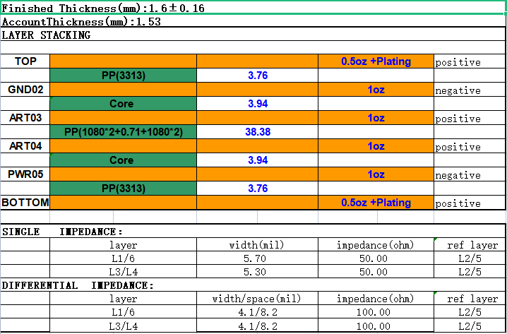
(dummy eight layers)
At this point we find that the 50om single-ended line width of the bottom layer is 5.7mil, the 100om differential line width is 4.1mil/8.2mil, the 50om impedance single-ended line width of the inner layer is 5.3mil, the 100om differential spacing is 4.1mil/8.2mil
This line width for conventional design is generally satisfied, then we can compare the two stacks, you will find that the difference between them is that the core is thinner, and then one or two layers and five or six layers of pp sheet also become thinner, core board and core board between the two sides of an additional core board without copper foil, then generally this stack we call "false eight layers ".
After understanding the differences between them then we can also summarise the advantages and disadvantages between them.
1, in the case of the need for impedance, we use the false eight-layer design can reduce our design line width, so as to meet our design requirements.
2, in the case of the third and fourth layers of the six-layer board laminated alignment using false eight-layer design can reduce the crosstalk between the third and fourth layers, because the third and fourth layers are adjacent to each other, if they are to be routed, the two layers are too thin between them will produce crosstalk, affecting the quality of the signal, so our false eight-layer design increases the distance between the two, crosstalk will be relatively small, but we also need to Note that, in the case of adjacent wiring layers, we need to use "vertical wiring", that is, a layer of alignment to take the horizontal, another layer to take the vertical.
3, due to the increase in materials and thus our costs will also be correspondingly higher, false eight layers is more expensive than six layers, but cheaper than eight layers.
The above is the knowledge to be introduced, I believe that after reading the completion of what is false eight layers also have a basic concept.
