How to effectively remove gold layer oxides or contaminants to facilitate bonding?
How to effectively remove gold layer oxides or contaminants to facilitate bonding?
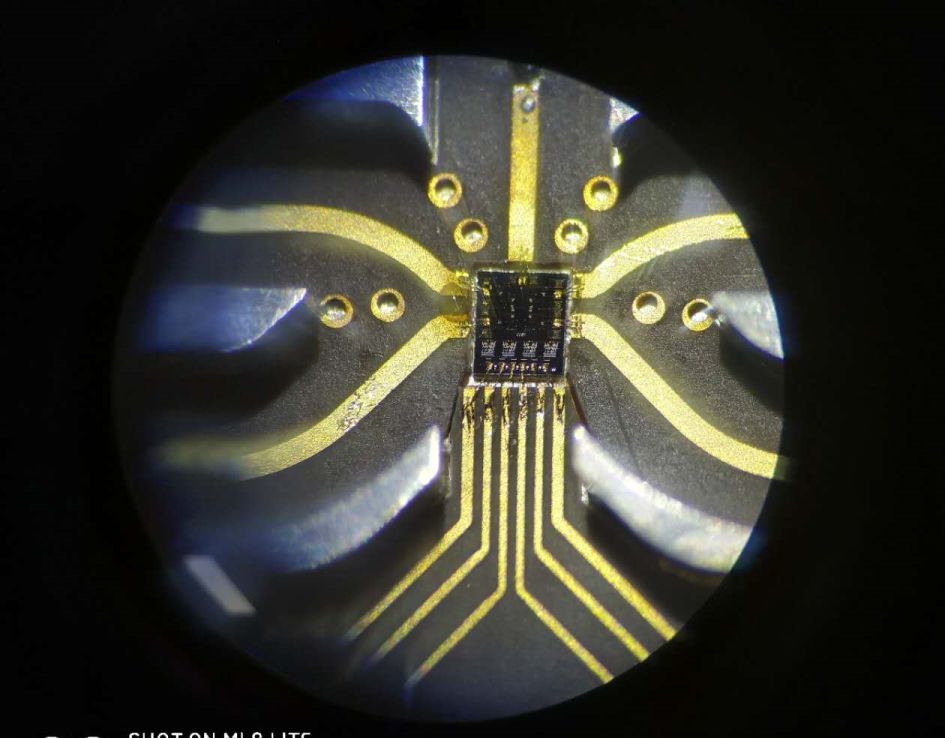
Jane: Teachers, how to effectively remove the oxide or contaminants of the gold layer to facilitate bonding
Liu Haiguang: Low-temperature plasma can effectively break the molecular bond between non-metal and metal
Jane: Is it cleaned by plasma cleaning machine before bonding? @Liuhaiguang
Liu Haiguang: Yes, this process should be popularized
Jane: Teacher Liu, for microstrip boards, what kind of gold plating is generally better? We require 2-3um gold layer, is it gold plating, immersion gold or nickel-palladium gold? Many microstrip lines on our boards are difficult to bond!
Liu Haiguang: Generally, gold plating and immersion gold need to be activated again or activated multiple times before they can continue to thicken..., the gold will be contaminated or the gold layer itself will carry some non-metallic components for a long time. Thick gold is a requirement for the line rather than the bonding point. This must be understood. Thick gold is easier to bond to gold. This is also one aspect@Jane
Liao Xiaobo: Gold is a highly corrosion-resistant metal, and theoretically there is no "oxidation" problem. The so-called "nickel-gold oxide film" generally refers to the oxidation of the underlying nickel plating due to its porosity when the gold plating is less than 1.5 microns. Plasma cleaning is very effective in removing organic matter on the surface of the plating, but it is not sufficient to reduce the oxide of metal nickel. Therefore, the effect of using plasma cleaning to restore the solderability of component terminals and leads may be random. In essence, it is not the removal of nickel oxides, but the reason for enhancing the effectiveness of flux in solder paste or solder wire after removing organic pollutants. Organic pollution is one of the reasons that affect the bonding strength of gold wires.
The effect of removing organic pollutants with plasma technology is very effective. Among them, vacuum plasma treatment is more effective than atmospheric plasma. But to clarify a concept, it does not mean that because plasma cleaning has a good decontamination effect, it can be used to replace flux cleaning @Jane
Jane: Thank you, teacher, what solvent is generally used to remove gold layer pollutants? There is no cleaning machine at present
Liao Xiaobo: The gold wire bonded printed circuit board pads and component leads and terminal plating must be more than 99.99% pure gold (commonly known as "soft"), and cannot be hard gold containing 0.0X% cobalt or nickel, antimony and other elements (commonly known as "wear-resistant gold"). As mentioned above, there are roughly two types of pollutants on the surface of the gold layer, organic pollutants and nickel oxides. When the thickness of the gold layer is greater than 2um, there is almost no nickel oxide, so the object of "cleaning" is mainly organic pollutants. To remove the pollutants on this gold layer, it is a very simple matter in the surface treatment process to use water-based cleaning agents to clean it. However, this water-based cleaning requires immersing the components in the cleaning solution and rinsing them multiple times after immersion, which is almost incredible for many components. Therefore, I say that vacuum plasma cleaning is the most practical cleaning method. @Jane
george tsao: You require the thickness of gold to be 2 to 3um. Have you actually measured the thickness? Which one are you currently using? Immersion gold? Also confirm that the thickness of gold is within the standard value, otherwise the situation will be completely different. If necessary, you can use EDS on the surface of the gold layer for reference
Jane: OK, the board is made by an external factory. We only asked for the thickness of the gold, but we didn't measure it specifically. The main reason is that it is difficult to bond and wire the microstrip line of the board. @george tsao
Liao Xiaobo: If I remember correctly, the aerospace standard requires the thickness of the gold plating layer for wire bonding to be above 0.8um. Products in other industries that do not emphasize reliability requirements seem to be above 0.5um. The gold plating on the microstrip line must also be software! @Jane
Jane: As shown below: Sometimes you have to scrape off some of the microstrip bonding area and plate it with soft gold
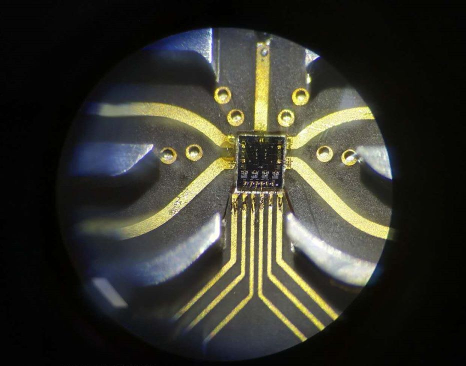
george tsao: Suspicious? This wire bonding point is ugly... a good gold layer shouldn't be like this
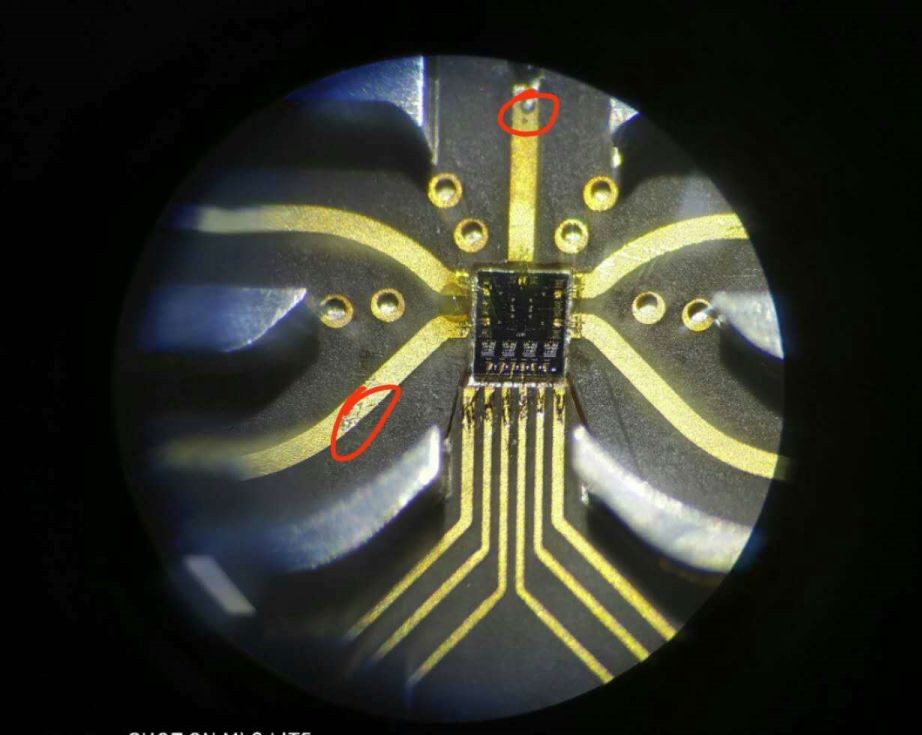
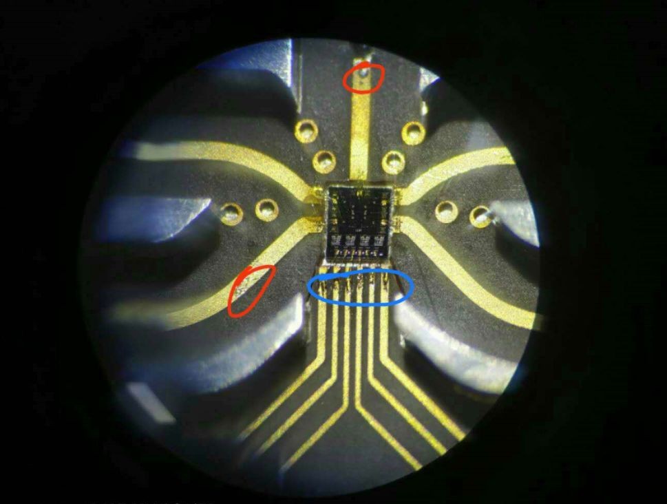
Jane: There are many defects in itself. During the experimental stage, the teacher was more careful and the picture was caused by welding
george tsao: A good gold layer shouldn't be like this @Jane
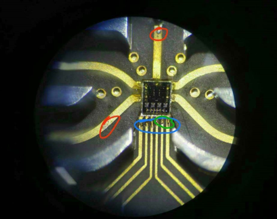
Jane: This gold layer has been scraped, so it looks like that. The purpose is to verify the indicators first. If you don't scrape, you can't bond the gold wire. Of course, the defect is too big
george tsao: Go and do EDS quickly and use the original unscratched one. The problem may be more serious than you think. Do more points @Jane
Liu Haiguang: Will the die bonding use a higher temperature? The placement time from die bonding to bonding will affect the quality of the bonding interface @Jane
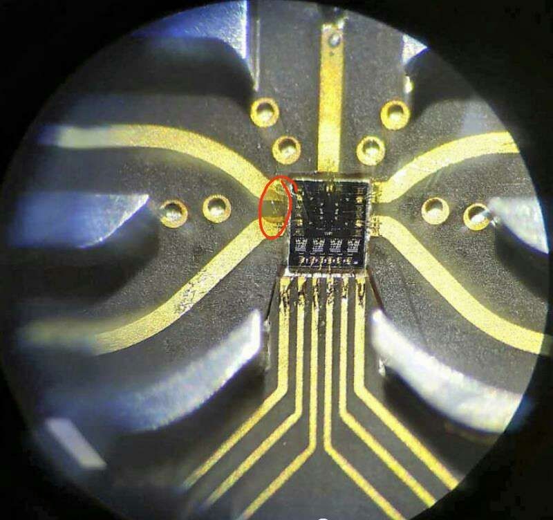
Jane: Bonding ultrasonic power, time, these parameters are set, preheating at 130℃ for bonding @Liu Haiguang
george tsao: It’s just that this area is not obvious, so it’s more accurate to look at EDS, as shown below:
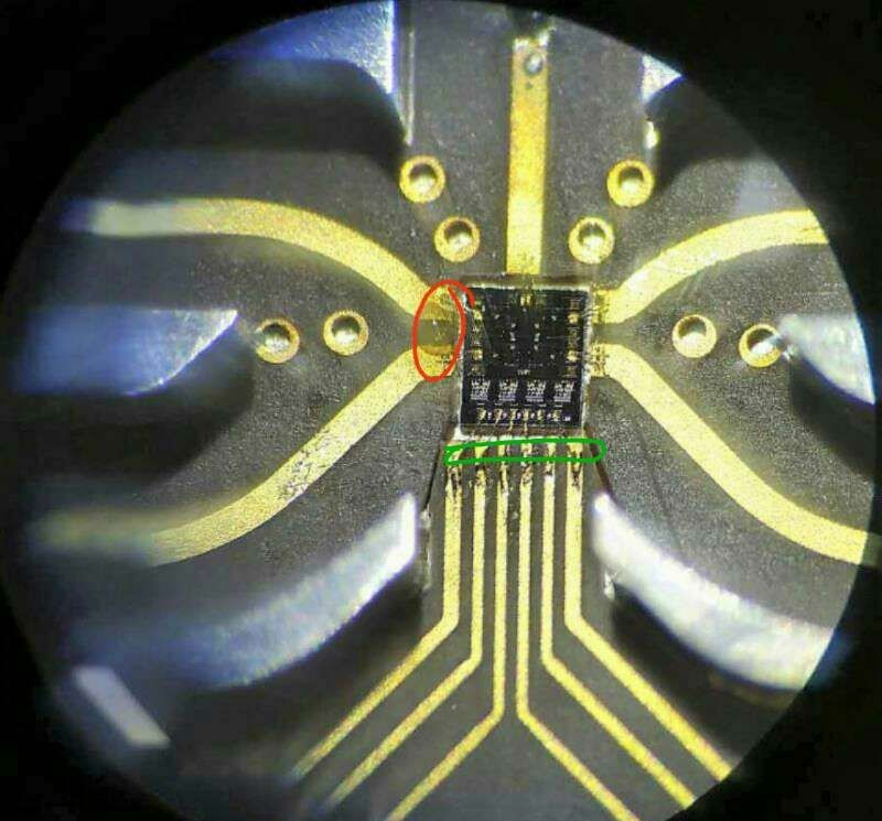
Jane: Teacher, look carefully, that is the flux @george tsao
Liao Xiaobo: If you don’t understand the mechanism of “why scraping can only be bonded”, it’s not a solution to scrape like this for a long time! It’s better to follow Teacher Cao’s advice and make an analysis. The appearance of the bonding synthesis photo is really a bit horrible. Do you confirm that it is reliable? @Jane
Jane: Yes, so we have asked the PCB factory to record the gold thickness measurement, because the gold layer was scraped, the underlying plating layer was exposed to the outside, and the bonding strength was affected. The gold wire fell off after this vibration! We are testing the indicators, and the national military standard requires at least 3g, so we have to test and verify in the end, otherwise it will not be used in the product
Liao Xiaobo: How thick is the gold layer after "scraping"? You all have no idea, but you dare to press weld in batches. Do you think that "it's OK as long as it's visually welded"? Or if there is no problem after a test, it is called "no problem"? Manual "scraping" of the plating layer, up and down, how to ensure that the thickness of the "remaining" gold plating layer after "scraping" is greater than the minimum thickness required by the process specification? For your gold-plated board, before welding, immerse the bare board in a citric acid aqueous solution (0.5 g to 1 g/L OP emulsifier) prepared with deionized water (or distilled water) at a temperature of 50℃ to 60℃ and a concentration of 40 g to 60 g/L for 2 to 3 minutes, then rinse it with tap water, and then immerse it in deionized water at 85±5℃ for tens of seconds. Take it out and dry it to remove moisture. The organic dirt on the surface of the coating should be removed. If necessary, brush the surface of the coating with a brush after soaking. @Jane
Jane: The teacher criticized that, so we have to analyze the reason why the board cannot be bonded after it comes back. The square edge of the board is cut by laser, and sometimes it will turn black. We are already rectifying it.
Liu Haiguang: First confirm the surface quality of the incoming material, measure the tensile force after bonding a few lines..., and do another comparison after solidification..., distinguish the problems of the incoming material and the process first, and then talk about countermeasures. Solder paste heating and flux contamination are not clean. For 3G and above, high-temperature silver glue protection can be applied, and the bonding position is staggered. @Jane
george tsao: Let's do something we did in the past that was unscientific. Take a piece of eraser that can erase ballpoint pen ink, like a leather eraser, and wipe the surface of the gold layer. Then wire it or even use a soldering iron to add solder. It's just a test. Don't rub too hard to avoid wiping off the gold layer. But it's still the same sentence. EDS, using a soldering iron is purely for observation. The condition of tinning or gold being eaten, and the problem of the bottom layer @Jane
Liu Haiguang: Under normal circumstances, gold will not be wiped off, glass fiber will not be wiped off, so much flux does not need to be processed, EDS does not need to be applied, a lot of O and C, EDS is only effective for incoming materials, surface contamination is better to use FTIR, because what is wiped off is the part that FTIR is good at detecting
Liao Xiaobo: Since gold elements do not have their own catalytic oxidation-reduction properties like copper elements, most of the current commercial chemical gold plating processes are the displacement reaction deposition processes introduced in junior high school chemistry, that is: when the nickel plating on the leads and terminals of the components contacts the gold ions in the solution, The gold ions will be replaced by nickel atoms and evenly covered (chemically deposited) on the surface of the nickel layer in the form of an atomic coating structure. When the nickel layer is completely covered by gold atoms, the replacement reaction should be completed. The thickness of such an immersion gold coating is essentially determined by the size of the gold crystal particles, and the maximum thickness is difficult to exceed 0.15 microns. The gold-plated layer of the microstrip line is mainly used to transmit microwave signals, and its thickness requirement is usually greater than 1um. Obviously, such a gold coating thickness can only be obtained by electroplating.
Jane: Thank you very much for the guidance of the three teachers, thank you


