PCB design high speed analogue input signal routing methods and rules
This article mainly details the PCB design high-speed analog input signal alignment, firstly, introduces the PCB design high-speed analog input signal alignment method, followed by the elaboration of the nine rules on PCB design high-speed analog input signal alignment, the specific follow me to understand.PCB design high-speed analog input signal alignment method
The wider the line width, the stronger the anti-interference capability, the better the signal quality (the impact of skin effect). But at the same time to ensure that the 50Ω characteristic impedance requirements. With a normal FR4 plate, the impedance of a 6MIL line width is 50 Ω. This obviously does not meet the requirements of the signal quality of high-speed analogue inputs, so we generally use a hollow GND02, so that it is referenced to the ART03 layer. This allows differential signals to be counted up to 12/10 and single lines up to 18MIL. (Note that there is no point in widening the line width beyond 18MIL)
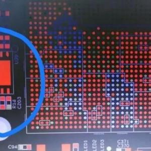
The CLINEs highlighted in green in the diagram are the single line and differential high speed analogue inputs referencing the ART03 layer. In doing so there are a number of details to be worked out.
(1) The analogue part of the TOP layer needs to be wrapped in ground treatment, as shown above. It should be noted that the distance from the copper cladding to the analogue input CLINE needs to be 3W, i.e. the AIRGAP from the edge of the copper cladding to the CLINE is twice the line width. According to some electromagnetic theory calculations and simulations, the magnetic and electric fields of the signal lines on the PCB are mainly distributed within the range of 3W. (Interference noise by surrounding signals is less than or equal to 1%).
(2) The GND copper laying in the positive layer of the analogue area also needs to be isolated from the surrounding digital area, i.e. all layers are isolated.
(3) The GND02 hollowing process, under normal circumstances we usually hollow out this area completely, so the operation is relatively simple and there is no problem. But considering the details or in order to do better, we can just hollow out the lower part of the analogue input alignment, which is of course the same as the TOP layer, the 3W area. This will ensure both the signal quality and the flatness of the board. The result of the treatment is as follows.
This allows the return path of the high-speed analogue input signal to be rapidly reflowed at the GND02 layer. That is, the analogue ground return path becomes shorter.
(4) Irregularly punching a large number of GND holes around the high-speed analogue signal, so that the analogue signal is rapidly returned. It can also absorb noise.
PCB design rules for high-speed analog input signal routing
High-speed PCB signal routing rules inventory
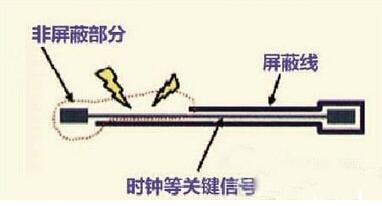
Rule one: high-speed PCB signal alignment shielding rules in the high-speed PCB design, the clock and other key high-speed signal lines, the alignment needs to be shielded processing, if not shielded or only shielded part, will cause EMI leakage. It is recommended that shielded lines, every 1000 mil, punched holes to ground.
PCB design high-speed analog input signal alignment methods and rules
Rule two: high-speed signal alignment closed-loop rules
Due to the increasing density of PCB boards, many PCB LAYOUT engineers in the process of alignment, it is easy to make a mistake, that is, the clock signal and other high-speed signal network, in the multi-layer PCB alignment when the results of the closed-loop, such a closed-loop results will produce a loop antenna, increasing the radiation intensity of EMI.
PCB design high-speed analog input signal alignment methods and rules

Rule three: high-speed signal alignment open-loop rules
Rule two mentions the closed loop of high-speed signals will cause EMI radiation, however, open loop will also cause EMI radiation.
Clock signals and other high-speed signal networks, in the multi-layer PCB alignment once the result of open-loop, will produce a linear antenna, increasing the radiation intensity of EMI.
PCB design high-speed analog input signal alignment methods and rules

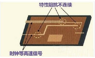
Rule four: the characteristic impedance of high-speed signals continuous rules
High-speed signals, switching between layers must ensure the continuity of the characteristic impedance, otherwise it will increase the radiation of EMI. In other words, the width of the wiring of the same layer must be continuous, and the impedance of the alignment of different layers must be continuous.
PCB design high-speed analog input signal routing methods and rules
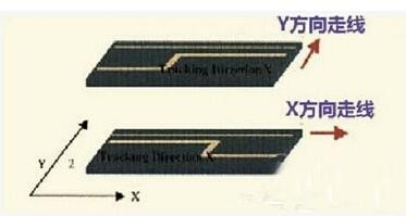
Rule 5: high-speed PCB design wiring direction rules
Adjacent to the two layers of the alignment must follow the principle of vertical alignment, otherwise it will cause crosstalk between the lines, increasing EMI radiation.
In short, the adjacent wiring layer to follow the horizontal and vertical wiring direction, vertical wiring can inhibit the crosstalk between lines.
PCB design high-speed analog input signal alignment methods and rules
Rule six: topology rules in high-speed PCB design
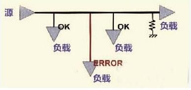
In high-speed PCB design, the control of the characteristic impedance of the circuit board and the design of the topology in the case of multiple loads directly determines the success or failure of the product.
The diagram shows a daisy-chain topology, generally used in the case of a few Mhz for the benefit. High-speed PCB design is recommended to use a star-shaped symmetrical structure at the back end.
PCB design high-speed analog input signal alignment methods and rules
Rule 7: Resonance rules for the length of the alignment
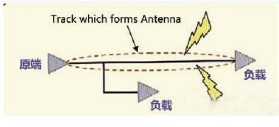
Check whether the length of the signal line and the frequency of the signal constitutes a resonance, that is, when the wiring length is an integer multiple of the signal wavelength 1/4, this wiring will produce resonance, and the resonance will radiate electromagnetic waves, generating interference.
PCB design high-speed analogue input signal routing methods and rules
Rule 8: Reflow path rules
All high-speed signals must have a good return path. As far as possible to ensure that the clock and other high-speed signals have the smallest possible return path. Otherwise it will greatly increase the radiation, and the size of the radiation and the signal path and the area surrounded by the return path is proportional.
PCB design high-speed analogue input signal alignment methods and rules
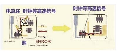
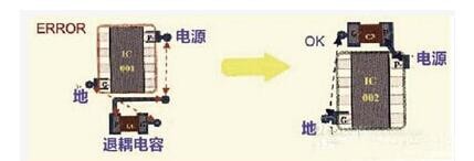
Rule 9: Decoupling capacitor placement rules for devices
The placement of decoupling capacitors is very important. The decoupling effect cannot be achieved at all if they are not placed properly. The principle is: close to the power supply pins, and the capacitor's power supply alignment and ground line surrounded by the smallest area.
PCB design high speed analogue input signal routing methods and rules
