What reinforcement measures can be taken from a process perspective while a QFN packaged chip fails during environmental testing?
What reinforcement measures can be taken from a process perspective while a QFN packaged chip fails during environmental testing?
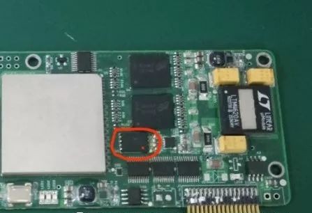
Cong Fei: Experts, I have a question: During environmental testing, a circuit board product failed during vibration or temperature cycle. It was located at the chip position of a QFN package, and after preliminary analysis, it was found to be a stress concentration area. Now we are not allowed to revise the design. We want to take reinforcement measures from a process perspective. Do you experts have any good suggestions? The board is relatively thin, 1.6 thick
Wang Peiheng: This board with K7 chip should be an auxiliary board for automotive electronics or military products. Except for the sealant around the edges, other solutions may not be acceptable for high and low temperature failure. Find Loctite or other glue suppliers to use black glue or sealant with low expansion coefficient to resist high and low temperatures to solve this problem
Cong Fei: Now we want to improve the shock resistance of the faulty chip from a process perspective. It is said that point glue potting is acceptable. I just want to ask if there is any experience to share in this regard
Wang Peiheng: If the LTM module is not moved out to resist the high temperature of reflow soldering during production, the process should be lead-containing. The LTM welding temperature cannot exceed 240 degrees, otherwise a short circuit will occur. In addition, arrange to upload pictures of the material DAP and PCB pads
Cong Fei: This chip is from Micron, using lead-containing welding technology. The chip and board have been analyzed for failure. The conclusion is no problem. The picture is as follows:
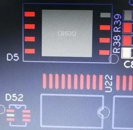
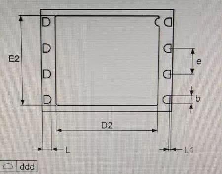
Wang Peiheng: This temperature should be the stand at the bottom of the material during welding High and low temperature failure caused by insufficient standoff. The steel mesh steps to 0.15MM. If the solder paste coverage rate at the grounding position meets 80%, there should be no such problem. QFN is connected to the PCB through solder paste. This connection is critical to the control of solder paste volume. This failure control standoff is controlled at about 50um.
Cong Fei: The steel mesh adopts a well-shaped window. The transfer rate should meet the requirements. I have suspected welding problems before. The steel mesh thickness is 0.13
Wang Peiheng: It should be its problem. You will know after making a batch of steps. There is no problem with your red ink and slicing.
Cong Fei: It should be on the pin, but the failure analysis conclusion says that there is no problem. There is another position on this board and the same package. There has been no problem. I have done it in a professional institution Destructive analysis
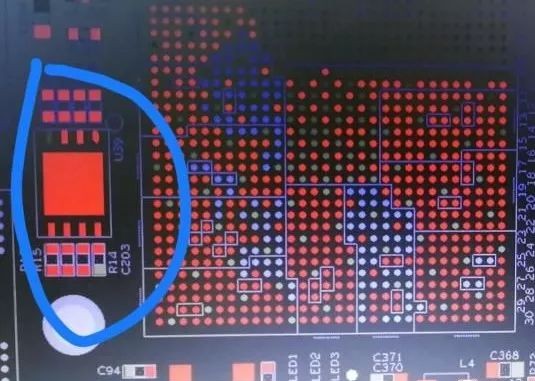
Li Hua: It should be caused by insufficient grounding leading to insufficient heat dissipation. The small foot welding can be strengthened by opening the steel mesh extension. I had a grounding of only 65% at one time, and the heat dissipation was insufficient and burned. Later, I asked the designer and he said it should reach more than 80%. After changing the steel mesh, it was ok. Stress concentration, it should be the BGA next to it that died first @Cong Fei
Wang Peiheng: Thickening can solve this problem
george tsao: First confirm whether the problematic solder joint is in this area @Cong Fei
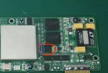
Cong Fei; Yes, Mr. Cao, it is all in this area
george tsao: The stress concentration area of the board, the solder joint is on the extension line of this area, try to add hardening glue in the green area, more amount, to prevent stress from passing through the solder joint, and cut the glue area in front of the solder joint to bypass it. However, be careful when applying glue. The width of the glue should not cross the BGA Colony area, avoid stress transfer to colony (see the following two pictures)
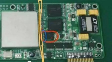
Chen Zhenghao: "Vibration or temperature cycle failure", locate QFN. What is the fault of QFN? If the phenomenon is not clear, reinforcement measures are proposed, and "zeroing" is unreasonable. What problems of QFN need to be accurately located. For example, is it a pin welding problem or a center ground pad welding problem? Is it a problem of solder joint welding strength temperature or excessive void rate of ground surface? Is it temperature that causes chip damage or vibration that causes solder joint cracking? First of all, the positioning must be accurate. If the ground pad has low solder penetration and poor heat dissipation, causing chip thermal damage, reinforcement will not work. In addition, QFN is in the stress zone. If the thickness of the board does not match the length and width, causing the board to deform and the warpage not meeting the requirements, reinforcement will not work. Design always relies on technology, but technology is not omnipotent.
Liao Xiaobo: Mr. Chen, I have a deeper understanding. It seems that the cause of this case is indeed the poor stress resistance of the QFN chip with that packaging structure. First, software simulation confirmed that the fault occurred in the area with the greatest stress on the board; second, my colleagues had encountered similar problems with chips of this packaging form and specification many times, and finally confirmed that it was caused by cracking of the bonding points in the chip due to stress. They agreed with the analysis unit that the stress resistance of QFN with this packaging size specification is indeed weak. As the saying goes, if the damage is inside the embankment, the damage is made up outside the embankment. Although the use of adhesive technology can make up for the weakness of the chip's poor stress resistance, it will also cause new adhesive curing stress and stress imbalance caused by improper adhesive application methods. I once suggested to the questioner to use low-stress epoxy glue, and they said that they had tried it and it did cause stress damage. In the end, we all agreed that we could only use silicone rubber adhesive to "reinforce" @Chen Zhenghao
Chen Zhenghao: As for the above-mentioned QFN device problem, it can be clearly seen that it is not a process problem, but a chip reliability problem and incorrect design (wrong installation position design, QFN design in a high stress area), and there is a very likely design error in the length, width and thickness ratio. For this type of double-material design error, hoping to solve it through various "reinforcements" is like "farting with pants on", which will cause endless troubles @Liao Xiaobo
Chen Zhenghao: Let's analyze it in depth. The designer "used software simulation to confirm that the fault occurred in the area with the highest stress on the board, and finally confirmed that it was caused by the stress cracking of the bonding point in the chip, and the stress resistance of QFN with this package size specification is indeed weak. As shown in Figure 1
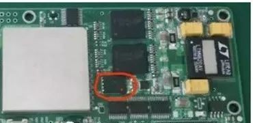
From Figure 1, we can be sure that the length, width and thickness design of this circuit board do not meet the standard requirements. The location of QFN is at the "cliff" of the board-high stress, and it is likely that not only the QFN device is damaged. For this kind of board with mismatched thickness and length and width, coupled with unreasonable component layout design, it is easy to produce high stress areas. The warpage of the circuit board before welding may have exceeded the tolerance, and the warpage after welding will definitely exceed 0.5. In this case, the QFN in the high stress area is bound to be damaged, which is the main reason. In response to the above problems, the design should take "reinforcement" measures, that is, Reinforce the board in the length direction - add reinforcing ribs, as shown in Figure 2.

The length, width and thickness design of the circuit board do not meet the standard requirements. QFN is installed in the high stress area, which is the main reason for the stress cracking of the bonding points in the chip.
The vibration resistance of QFN devices also needs to be analyzed. One of the main reasons why we use BTC devices is that BTC devices have a low installation height and strong vibration resistance. However, the vibration resistance of any device has a range. If the device is incorrectly designed in a high stress area that the device cannot withstand, it is not a reliability problem of the device, but a design level problem of the user. So I don’t think that bonding reinforcement can fundamentally solve the problem
Cong Fei: The design status is not allowed to be changed. At present, it is estimated that only glue can be used for reinforcement. I will try it first and ask if there is any problem. Thank you for your advice


