FR-4 PCB manufacturing process-Surface Treatment
In the manufacturing process of PCB (Printed Circuit Board), the surface treatment process plays a crucial role and has a profound impact on the performance, reliability and subsequent assembly process of PCB.Let's first talk about FR-4 PCB manufacturing process bare copper clad laminates. The cost of bare copper clad laminates is relatively low, and their surface is relatively flat. Under the ideal condition of no oxidation, the soldering performance is good. However, it has significant drawbacks. Bare copper clad laminates are extremely vulnerable to environmental factors such as acids and humidity, with poor stability and unable to be stored for a long time. Once unpacked, they must be used within a short period of 2 hours, otherwise the copper surface will start to oxidize. In addition, due to its insufficient anti-oxidation ability, bare copper clad laminates cannot be applied in the manufacturing of double-sided boards because the second side often oxidizes after undergoing the first reflow soldering process.
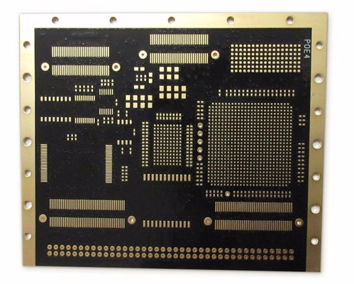
FR-4 PCB manufacturing process Gold-plated boards also occupy a position in PCB surface treatment. The selection of gold as the plating layer is mainly based on two key considerations: one is to greatly optimize the convenience of soldering, and the other is to endow it with excellent anti-corrosion performance. Even the gold fingers of memory modules that have experienced many years of use can still maintain their original shiny luster. However, gold-plated boards also have their undeniable shortcomings, that is, the high cost. The use of gold plating layers makes them account for nearly 10% of the cost of the circuit board, which to a certain extent limits their wide application in cost-sensitive applications.

FR-4 PCB manufacturing process the hot air solder leveling (HASL) process is widely used in PCB manufacturing. This process involves immersing the PCB in molten tin (lead) solder and then leveling (blowing) it using heated compressed air to form a coating layer on the PCB surface that is resistant to copper oxidation and provides good soldering performance. The HASL process can be further subdivided into leaded HASL and lead-free HASL. In the current market environment, leaded HASL occupies a large market share due to its relatively low price. However, with increasingly strict environmental protection requirements, lead-free HASL is expected to gain wider application in the future due to its more environmentally friendly characteristics.
FR-4 PCB manufacturing process the organic solderability preservative (OSP) treatment is another common PCB surface treatment method. Its principle is to generate an organic film on the clean bare copper surface through a chemical method. This film has excellent anti-oxidation, thermal shock resistance and moisture resistance, and can effectively protect the copper surface in a normal environment and prevent it from continuing to rust (such as oxidation or sulfidation, etc.). More importantly, during the subsequent soldering process, when encountering high temperatures, this protective film can be easily and quickly removed by the soldering flux, thereby enabling the clean copper surface to closely combine with the molten solder in a very short time to form a firm and reliable solder joint.
FR-4 PCB manufacturing process the full-board nickel-gold plating process also holds an important position in PCB surface treatment. This process first plates a layer of nickel on the conductors on the PCB surface and then covers it with a layer of gold. The main purpose of nickel plating is to prevent the diffusion between gold and copper. Currently, electroplated nickel-gold mainly falls into two categories: soft gold plating (pure gold, with the gold surface looking less shiny) and hard gold plating (with a smooth and hard surface, wear resistance, containing other elements such as cobalt, and the gold surface looking brighter). Soft gold is mainly used for wire bonding during chip packaging; hard gold is mainly used for electrical interconnection at non-soldering locations to provide good electrical conductivity and wear resistance.
FR-4 PCB manufacturing process the immersion gold process is also favored in PCB manufacturing. By depositing a thick and electrically good nickel-gold alloy on the copper surface, long-term and effective protection can be provided for the PCB. The immersion gold process also shows excellent environmental tolerance and can maintain the performance stability of the PCB even under complex and changeable environmental conditions. In addition, the immersion gold process is also conducive to lead-free assembly and can effectively prevent the dissolution of copper.
FR-4 PCB manufacturing process the immersion tin process has unique advantages. It can form a flat copper-tin intermetallic compound on the copper surface. This feature enables the immersion tin to have good solderability similar to hot air solder leveling while avoiding the flatness problem faced by hot air solder leveling. However, immersion tin boards have certain limitations in storage and cannot be stored for too long, and during assembly, the order of immersion tin must be strictly followed.
FR-4 PCB manufacturing process the immersion silver process also has its specific application scenarios in PCB surface treatment. It lies between organic coating and chemical nickel/gold immersion, and the process is relatively simple and fast. Even when exposed to hot, humid and contaminated environments, the silver layer can still maintain good solderability, but the surface luster may be lost. However, the immersion silver process also has its shortcomings. Since there is no nickel layer under the silver layer, it is inferior to the chemical nickel/gold immersion process in terms of physical strength.
FR-4 PCB manufacturing process the chemical nickel-palladium-gold process is a more advanced surface treatment technology. Compared with the immersion gold process, the chemical nickel-palladium-gold process adds an additional layer of palladium between the nickel and gold layers. The presence of the palladium layer can effectively prevent the corrosion phenomenon caused by the displacement reaction and fully prepare for the subsequent immersion gold step. The gold layer is closely covered on the palladium layer, providing a high-quality contact surface for the PCB and further improving the performance and reliability of the PCB.
FR-4 PCB manufacturing process the electroplated hard gold process is usually used to enhance the wear resistance of the product and increase the number of insertions and withdrawals. By plating a hard gold layer on the PCB surface, the durability of the PCB under frequent insertions, withdrawals and frictions can be significantly enhanced, thereby meeting the requirements of some application scenarios with high mechanical performance requirements.
In conclusion, the surface treatment processes in PCB manufacturing are diverse, and each process has its unique performance characteristics, advantages and application scopes. In the actual PCB manufacturing process, it is necessary to comprehensively consider various factors such as the specific requirements of the product, performance requirements, cost budget and environmental protection regulations, and carefully select the most suitable surface treatment process to ensure that the final manufactured PCB can meet the strict requirements of high quality and high performance for electronic devices.


