Manufacturing process of PCB-inner layer dry film
In the manufacturing process of PCB (Printed Circuit Board), the inner layer dry film is a crucial step, which precisely defines the circuit pattern for the subsequent etching process. The following is a detailed introduction to the manufacturing process of the inner layer dry film.
First is the PCB manufacture inner layer dry film pre-treatment stage. This step is like making fundamental preparations for the upcoming important processes. The substrate of the inner layer of the PCB undergoes a strict cleaning process. Through methods such as chemical cleaning or physical brushing, contaminants such as oil stains, dust, and oxides that may exist on the surface are completely removed. Because even extremely tiny contaminant particles may lead to poor adhesion of the dry film in the subsequent processes and affect the accuracy and quality of the circuit pattern. After cleaning, to further enhance the adhesion between the dry film and the substrate, the surface of the substrate is micro-roughened. This is usually achieved through methods such as chemical etching or mechanical grinding, creating tiny concave and convex structures on the substrate surface. This micro-roughening not only increases the surface area but also provides more physical anchor points for the dry film, ensuring that the dry film can firmly adhere to the substrate.

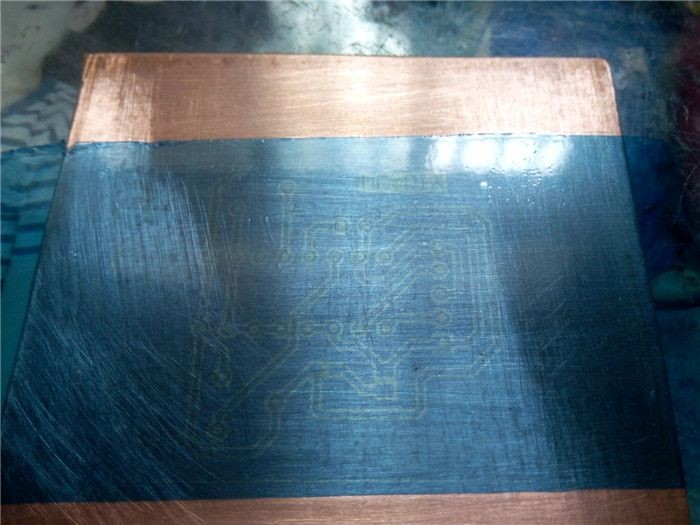
After the PCB inner layer dry film lamination is completed, the exposure step follows. This step is like giving the "soul" to the dry film, determining the accuracy of the final circuit pattern. The substrate with the adhered dry film is precisely aligned with the pre-prepared film. The film has a specific circuit pattern made according to the design requirements. Its transparent areas correspond to the parts where the dry film needs to be cured, while the opaque areas protect the underlying dry film from exposure. Then, it is irradiated with a high-intensity ultraviolet light source. Under the action of ultraviolet light, the photopolymerizable resist in the dry film undergoes a chemical reaction, and the molecular structure changes, thereby hardening the corresponding positions of the dry film. The exposure time and intensity need to be strictly controlled to ensure that the parts of the dry film that need to be retained are fully cured while avoiding adverse effects caused by excessive exposure.
After the PCB manufacturing inner layer drt film exposure is completed, the development process follows immediately. This step is like a well-planned "baptism" that leaves only the necessary parts. The exposed substrate is placed in a special developing solution, which is typically an alkaline solution. The dry film that has not been exposed to ultraviolet light will dissolve under the action of the developing solution, while the exposed and hardened dry film will resist the erosion of the developing solution, thereby clearly revealing the copper layer parts that need to be etched on the substrate, forming a precise prototype of the circuit pattern.
Finally, there is the PCB manufacturing inner dry layer inspection stage. This is a key quality control link to ensure the quality of the PCB inner layer dry film. Operators will use tools such as magnifying glasses and microscopes to carefully inspect the developed substrate. The focus is on the integrity of the dry film coverage, the clarity and accuracy of the pattern, as well as the presence of bubbles, wrinkles, residual undeveloped dry film, and other defects. If any issues are found, corresponding measures will be taken based on the severity of the defects. For minor defects, local repairs may be carried out, while for severe defects, processes such as re-lamination, exposure, and development may be required.
Through the above series of rigorous and fine PCB manufacturing processes of the inner layer dry film, a circuit pattern that meets the design requirements is successfully formed on the inner layer substrate of the PCB, laying a solid foundation for the subsequent etching, plating, and other processes, and ultimately achieving high-quality and high-precision PCB manufacturing.


