How to optimise switching power supply layouts by minimising thermal circuit PCB ESR and ESL?
[Read More] For power converters, a thermal circuit PCB layout with minimal parasitic parameters can improve energy efficiency ratios, reduce voltage ringing, and reduce electromagnetic interference (EMI). adi will discuss in this paper how to optimize the thermal circuit layout design by minimizing the equivalent series resistance (ESR) and equivalent series inductance (ESL) of the PCB. Influencing factors, including decoupling capacitor location, power FET size and location, and via arrangement, are investigated and compared in the paper. The results of the analysis are verified experimentally and effective methods for minimising PCB ESR and ESL are summarised.
Question.
Is it possible to optimise the efficiency of a switching power supply?
ANSWER.
Of course you can, minimising the PCB ESR and ESL of the hot loop is an important method to optimise efficiency.
Introduction
In this paper ADI discusses how to optimise the thermal circuit layout design by minimising the equivalent series resistance (ESR) and equivalent series inductance (ESL) of the PCB. Influencing factors, including decoupling capacitor location, power FET size and location, and via arrangement, are investigated and compared in the paper. The results of the analysis are verified experimentally and effective methods for minimising PCB ESR and ESL are summarised.
Thermal circuit and PCB layout parasitic parameters
The thermal loop of a switched-mode power converter is the critical high frequency AC current loop formed by the high frequency (HF) capacitor and the adjacent power FETs. It is the most critical part of the power stage PCB layout as it contains high dv/dt and di/dt noise components. A poorly designed thermal loop layout can produce large PCB parasitic parameters including ESL, ESR and equivalent parallel capacitance (EPC) which have a significant impact on the efficiency, switching performance and EMI performance of the power converter.
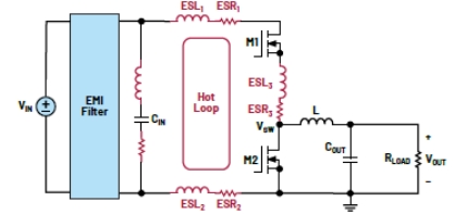
Figure 1. Buck converter with hot-loop ESR and ESL
Figure 1 shows the schematic of a synchronous buck DC-DC converter. The thermal loop is formed by the MOSFETs M1 and M2 and the decoupling capacitor CIN. the switching action of M1 and M2 generates high frequency di/dt and dv/dt noise. the CIN provides a low impedance path to bypass the high frequency noise component. However, parasitic impedance (ESR, ESL) exists within the device package and on the thermal circuit PCB alignment. The high di/dt noise through the ESL causes high frequency ringing and consequently EMI. the energy stored in the ESL is dissipated in the ESR, resulting in additional power loss. Therefore, the ESR and ESL of the hot loop PCB should be minimised to reduce high frequency ringing and improve efficiency.
Accurately extracting the ESR and ESL of the thermal loop can help predict switching performance and improve the thermal loop design. Both the package and PCB alignment of the device will affect the total parasitic parameters of the loop. This article focuses on PCB layout design. There are tools available to help users extract PCB parasitic parameters, such as Ansys Q3D, FastHenry/FastCap, StarRC, etc. Commercial tools such as Ansys Q3D provide accurate simulations, but are often expensive. The validity and accuracy of FastHenry/FastCap parasitic parameter extraction has been verified and compared with Ansys Q3D with consistent results2,3 . In this paper, FastHenry is used as a cost effective tool for extracting PCB ESR and ESL.
ESR and ESL of a hot-loop PCB versus decoupling capacitor position
This section investigates the effect of CIN position based on ADI's LTM4638 µModule® regulator demonstration board DC2665A-B. The LTM4638 is an integrated 20VIN, 15A buck converter module in a small 6.25mm × 6.25mm × 5.02mm BGA package. It offers high power density, fast transient response and high efficiency characteristics. A small high frequency ceramic CIN is integrated inside the module, although this is not sufficient due to the size of the module package. Figures 2 to 4 show three different thermal loops on the demo board that use an additional external CIN. the first is vertical thermal loop 1 (Figure 2), where CIN1 is placed on the bottom layer below the µModule regulator. the µModule VIN and GND BGA pins are connected directly to CIN1 via vias. these connections provide the shortest thermal loop path on the demo board These connections provide the shortest thermal loop path on the demo board. The second thermal circuit is the vertical thermal circuit 2 (Figure 3), where CIN2 is still placed on the bottom layer but moved to the side area of the µModule regulator. The result is that this thermal loop adds additional PCB alignment and is expected to have a larger ESL and ESR compared to vertical thermal loop 1. The third thermal loop option is the horizontal thermal loop (Figure 4), where CIN3 is placed close to the top layer of the µModule regulator. µModule VIN and GND pins are connected to CIN3 via the top copper layer without going through the vias. However, the width of the VIN copper on the top layer is limited by the arrangement of the other pins, resulting in a higher loop impedance than for vertical thermal loop 1. Table 1 compares the PCB ESR and ESL of the thermal loops extracted by FastHenry. as expected, vertical thermal loop 1 has the lowest PCB ESR and ESL.
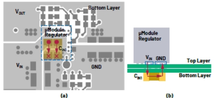
Figure 2. Vertical thermal loop 1: (a) top view and (b) side view
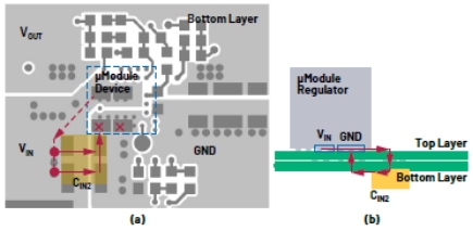
Figure 3. Vertical thermal circuit 2: (a) top and (b) side view
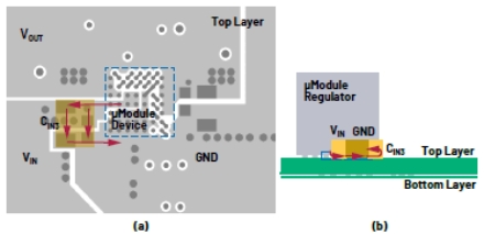
Figure 4. Horizontal thermal circuit: (a) top and (b) side view
Table 1. PCB ESR and ESL of different thermal loops extracted using FastHenry

To experimentally verify the ESR and ESL of the different thermal loops, ADI tested the efficiency and VIN AC ripple of the demo board during 12V to 1V CCM operation. Theoretically, the lower the ESR, the higher the efficiency, while the smaller the ESL, the higher the VSW ringing frequency and the lower the VIN ripple amplitude. Figure 5a shows the measured efficiencies. Vertical hot loop 1 is the most efficient as it has the lowest ESR. The difference in losses between the horizontal and vertical thermal loops 1 is also calculated based on the extracted ESR, which is consistent with the test results shown in Figure 5b. The VIN HF ripple waveform in Figure 5c was tested on the CIN. The horizontal thermal loop has a higher VIN ripple amplitude and lower ringing frequency, thus verifying a higher loop ESL than the vertical thermal loop 1. In addition, the horizontal thermal loop has a faster VIN ripple attenuation than the vertical thermal loop 1 due to the higher loop ESR. In addition, the lower VIN ripple reduces EMI, thus allowing the use of a smaller EMI filter.
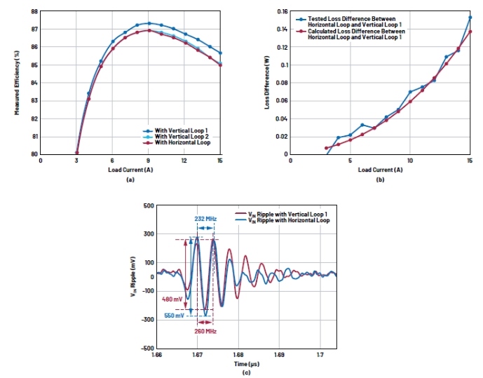
Figure 5. Demo board test results: (a) efficiency, (b) difference in losses between horizontal and vertical loop 1, (c) VIN ripple during M1 conduction at 15 A output
Hot Loop PCB ESR and ESL as a function of MOSFET size and location
For discrete designs, the arrangement and package size of the power FETs also have a significant impact on the hot-loop ESR and ESL. In this section ADI models and investigates a typical half-bridge thermal circuit using power FETs M1 and M2 and decoupling capacitor CIN. Figure 6 compares common power FET package sizes and placements. Table 2 shows the extracted ESR and ESL for each case.
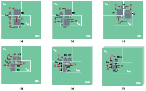
Figure 6. Thermal circuit PCB models: (a) 5mm × 6mm MOSFET in a straight line arrangement; (b) 5mm × 6mm MOSFET in a 90° shape arrangement; (c) 5mm × 6mm MOSFET in a 180° shape arrangement; (d) two parallel 3.3mm × 3.3mm MOSFETs in a 90° shape arrangement; (e) two parallel 3.3mm × 3.3mm MOSFETs in 90° shape with ground layer; (f) Symmetrical 3.3mm × 3.3mm MOSFETs on top and bottom layers in 90° shape.
Table 2. Thermal circuit PCB ESR and ESL extracted using FastHenry for different device shapes and locations

Cases (a) to (c) show three common power FET arrangements with 5mm × 6mm MOSFETs. the physical length of the thermal circuit determines the parasitic impedance. Compared to case (a), the 90° shape arrangement in case (b) and the 180° shape arrangement in case (c) have shorter loop paths, resulting in a 60% reduction in ESR and an 80% reduction in ESL. As the 90° shape arrangement shows advantages, further cases can be investigated based on case (b) to further reduce loop ESR and ESL. case (d) replaces a 5mm × 6mm MOSFET with two 3.3mm × 3.3mm MOSFETs in parallel. the loop length is further reduced due to the smaller MOSFET size, resulting in a 7% reduction in loop impedance. Case (e), where a ground layer is placed below the thermal loop layer, results in a further 2% reduction in thermal loop ESR and ESL compared to case (d). The reason for this is the creation of eddy currents on the grounding layer, which induce an opposite magnetic field, corresponding to a reduction in loop impedance. Case (f) constructs another thermal circuit layer as the grounding layer. If the two parallel MOSFETs are arranged symmetrically on the top and bottom layers and connected via vias, the reduction of the hot-loop PCB ESR and ESL is even more pronounced due to the parallel impedance. Therefore, the lowest PCB ESR and ESL can be obtained by arranging smaller sized devices in a symmetrical 90° shape or 180° shape on the top and bottom layers.
To experimentally verify the impact of the MOSFET arrangement, ADI's high efficiency 4-switch synchronous buck-boost controller demonstration boards LT8390/DC2825A and LT8392/DC2626A4 can be used. as shown in Figure 7a and Figure 7b, the DC2825A uses a linear MOSFET arrangement and the DC2626A uses a 90° shaped MOSFET arrangement. For a fair comparison, both demo boards were configured with identical MOSFETs and decoupling capacitors and tested under 36V to 12V/10A, 300kHz buck operation. Figure 7c shows the VIN AC ripple measured at the moment of M1 conduction. The lower amplitude and higher resonant frequency of the VIN ripple when using a 90° shaped MOSFET arrangement verifies that the shorter thermal circuit path results in a smaller PCB ESL. In contrast, the linear MOSFET arrangement has a longer thermal circuit and a higher ESL, resulting in a much higher VIN ripple amplitude and a lower resonant frequency. Higher input voltage ripple also leads to more severe EMI radiation according to the EMI test results of the Cho and Szokusha study4.
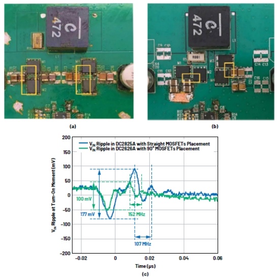
Figure 7. (a) LT8390/DC2825A thermal loop with MOSFETs arranged in a straight line; (b) LT8392/DC2626A thermal loop with MOSFETs arranged in a 90° shape; (c) VIN ripple waveform when M1 is on.
ESR and ESL of the thermal circuit PCB in relation to the via layout
The over-hole layout in the thermal circuit also has a significant impact on the circuit ESR and ESL. Figure 8 models a thermal loop using a two-layer PCB structure and a linear arrangement of power FETs. the FETs are placed on the top layer and the second layer is the ground layer. the parasitic impedance Z2 between the CIN GND pad and the M2 source pad is part of the thermal loop and is studied as an example. z2 is extracted from FastHenry. Table 3 summarises and compares the simulated ESR2 and ESL2 for different over-hole arrangements.

Figure 8. Thermal circuit PCB model with (a) 5 GND vias arranged close to CIN and M2; (b) 14 GND vias arranged between CIN and M2; (c) 6 more vias on GND based on (b); (d) 9 more vias on GND area based on (c).
In general, adding more vias will reduce the PCB parasitic impedance. However, the reduction in ESR2 and ESL2 is not linearly proportional to the number of vias. The most significant reduction in PCB ESR and ESL is caused by vias close to the pin pads. Therefore, for thermal circuit layout designs, several critical vias must be placed close to the CIN and MOSFET pads in order to minimise the high frequency circuit impedance.
Table 3. Extracted PCB ESR2 and ESL2 for thermal loops when using different via arrangements

Conclusion
To minimise PCB parasitic parameters, ADI has studied and compared thermal loop layout designs using different decoupling capacitor locations, MOSFET sizes and locations, and vias arrangements. Shorter thermal loop paths, smaller sized MOSFETs, symmetrical 90° shaped and 180° shaped MOSFET arrangements, and vias close to critical components all contribute to the lowest thermal loop PCB ESR and ESL.
