PCB manufacturing process-Pattern Plating
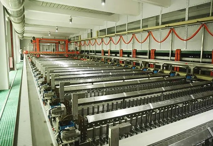
In the manufacturing process of PCB (Printed Circuit Board), pattern plating is an extremely crucial and delicate process. It mainly involves depositing a layer of copper, gold-nickel or tin of a specific required thickness on the copper-clad laminate that has undergone hole metallization treatment through electroplating, thereby laying a solid foundation for the performance and reliability of the PCB.First is the loading step in PCB manufacturing process pattern plating. This step may seem simple but actually requires the operator to be highly meticulous and patient. The copper-clad laminate that has completed hole metallization is carefully placed on the electroplating equipment to ensure that the position of the board is accurate and in good contact with the electrodes of the equipment. Any minor deviation may affect the uniformity and quality of the subsequent plating.
Next is the degreasing operation in PCB manufacturing process pattern plating. During the manufacturing and transportation of the board, the surface inevitably gets contaminated with oil and various impurities. The purpose of degreasing is to completely remove these contaminants and provide a clean and tidy adhesion surface for the subsequent plating layer. Special degreasing agents are usually used to decompose and dissolve the oil through chemical reactions.
After degreasing is completed, the washing step follows immediately in PCB manufacturing process pattern plating. This is to remove the residual degreasing agent on the surface of the board. If the degreasing agent remains, it will interfere with the subsequent plating process and affect the adhesion and uniformity of the plating layer. Washing is usually carried out by multiple sprayings or soakings to ensure that the board is thoroughly cleaned.

The micro-etching is the next important step in PCB manufacturing process pattern plating. By slightly etching the surface of the board, it is possible to further remove any possible oxide layers and minor flaws, while increasing the roughness of the board surface. In this way, the subsequent deposited plating layer can bond better with the board and improve adhesion.
After the micro-etching is completed, washing is performed again in PCB manufacturing process pattern plating. This step is to rinse off the residual micro-etching agent and prevent it from adversely affecting the subsequent plating process. The effectiveness of washing is directly related to the stability and reliability of the subsequent processes.
The pickling step in PCB manufacturing process pattern plating is also not to be ignored. After going through the previous steps, the surface of the board may form new oxide layers. Pickling can effectively remove these oxide layers and ensure that the surface of the board is clean and activated, fully preparing for the deposition of a high-quality plating layer.
Then comes the copper plating step in PCB manufacturing process pattern plating. This is one of the core steps in pattern plating. Under suitable current and plating solution conditions, copper ions are reduced and deposited on the surface of the board, forming a uniform and dense copper layer. This copper layer not only serves the function of conducting the circuit but also provides a good foundation for the subsequent processes.
After copper plating is completed, washing is performed in PCB manufacturing process pattern plating. This is to remove the residual copper plating solution on the surface of the board and avoid its interference with the subsequent processes. The thoroughness of washing is directly related to the quality of the subsequent tin plating and other processes.
The acid immersion step follows immediately in PCB manufacturing process pattern plating. The board is immersed in an acidic solution to further remove any newly formed oxide layers and maintain the activity and cleanliness of the board surface.
Next is the tin plating step in PCB manufacturing process pattern plating. A layer of tin is deposited on the copper layer. This layer of tin mainly serves to protect the copper layer from oxidation and at the same time improve the solderability of the board, facilitating the subsequent soldering and installation of electronic components.
After tin plating is completed, washing is performed again in PCB manufacturing process pattern plating. Thoroughly remove the residual tin plating solution to ensure that the surface of the board is clean and free of impurities.
Finally, there is the unloading step in PCB manufacturing process pattern plating. The operator carefully removes the board that has completed pattern plating from the electroplating equipment and places it in a designated position for subsequent process treatment.
The quality of pattern plating has a crucial impact on the performance and reliability of the PCB. Throughout the pattern plating process, it is necessary to strictly control the process parameters of each step, such as current density, plating time, solution temperature and concentration, etc. Only by ensuring the accuracy and stability of these parameters can the plating layer have a uniform thickness and strong adhesion, thereby meeting the high-performance and high-reliability requirements of the PCB in complex electronic devices.
At the same time, during the process of pattern plating in PCB manufacturing process, it is also necessary to attach great importance to environmental protection and safe operation. Most of the chemical solutions used in electroplating are corrosive and toxic. If not handled properly, it may cause serious pollution to the environment and harm to the health of the operators. Therefore, effective protective measures and strict environmental protection processing procedures must be adopted to ensure that the production process is both efficient and safe and environmentally friendly.
In conclusion, pattern plating is a complex and crucial process in PCB manufacturing, which requires precise operation, strict parameter control and a high degree of attention to environmental protection and safety in order to produce high-quality PCB products.


