FR-4 PCB Manufacturing process-Final inspection
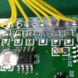
The final inspection in the PCB (Printed Circuit Board) manufacturing process is a crucial stage to ensure product quality and compliance with design specifications.The FR-4 PCB manufacturing process final inspection usually covers several aspects. Firstly, it is the appearance inspection, checking whether the PCB surface has scratches, stains, discoloration, uneven or missing plating, and other defects. It is also necessary to check whether the solder mask layer is complete and the character markings are clear and accurate.
Secondly, it is FR-4 PCB manufacturing process final inspection-the circuit connectivity inspection. Through professional testing equipment, it is detected whether the lines on the PCB conduct well and whether there are problems such as open circuits and short circuits. This is crucial for ensuring the normal function of the circuit.

Furthermore, it is FR-4 PCB manufacturing process the inspection of the aperture and aperture tolerance. Ensure that the sizes of mounting holes, vias, etc. comply with the design requirements and the tolerance is within the allowable range.
The basic parameters such as the number of layers, board thickness, and materials of the PCB will also be verified to confirm consistency with the design specifications.
In addition, FR-4 PCB manufacturing process final inspection a solderability test will be conducted to check the performance of the metal plating on the PCB surface during the soldering process, whether it is easy to tin and whether the soldering quality is good.
For PCBs with special requirements, such as high-frequency boards, high-frequency characteristics will also be tested, including signal transmission performance and impedance matching.
The results of the FR-4 PCB manufacturing process final inspection will determine whether the PCB is qualified and can be delivered for use. If problems are found, repair, rework, or even scrapping may be required. A strict final inspection helps improve the quality and reliability of the PCB and guarantees the performance and stability of electronic products.
In the FR-4 PCB manufacturing process final inspection during the PCB manufacturing process, common quality issues include:
1. Circuit defects:
- Open circuits: There are disconnected parts in the circuit, preventing normal current flow.
- Short circuits: Unexpected connections between circuits, causing current short circuits.
- Inconsistent line widths: Not in line with design requirements, which may affect current carrying capacity and signal transmission.
- Excessive or insufficient aperture sizes: Affecting component installation or inner layer connections.
- Rough hole walls: May lead to poor connections or affect signal transmission.
- Foreign substances or residues in the holes: Hindering electrical connections.
- Uneven plating: Some areas are too thick or too thin, affecting solderability and conductivity.
- Plating voids: Reducing the continuity and reliability of the plating.
- Discoloration or oxidation of the plating: Affecting appearance and solderability.
- Solder mask layer detachment or blistering: May cause short circuits or affect protection effects.
- Uneven thickness of the solder mask layer: Affecting subsequent assembly and soldering.
- Incomplete coverage of the solder mask layer: Exposing areas that should not be soldered.
- The length and width of the PCB do not meet the design requirements.
- The board edges are not smooth or have burrs.
- Fuzzy markings: Making it difficult to identify component positions and polarities and other information.
- Missing or incorrect characters: Leading to misjudgment during assembly and repair.
7. Layer delamination: Separation occurs between the inner layers of the PCB, affecting electrical performance and structural strength.
8. Warpage and deformation: The PCB bends or twists, which is not conducive to installation and use.
9. Foreign substance contamination: The PCB surface has contaminants such as dust, oil stains, and water stains.


