Analysis and discussion on the causes of IC solder joint falling off
Analysis and discussion on the causes of IC solder joint falling off
Shuai Shuai: Teachers, please help me look at the solder joints of the IC below. The IC fell off directly after opening the cover. What are the reasons?
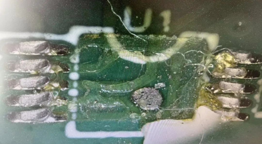
Liao Xiaobo: The biggest suspicion is not a false solder joint! It is a cold solder joint! Do you have a high-definition photo of the upper part of the chip pin that fell off? Use a Keyence 3D microscope to take a photo!
Shuai Shuai: The other devices on the board are all well soldered
Liao Xiaobo: Protect this sample and do not let it be mechanically damaged or organically contaminated. Send it for an X-ray fluorescence spectrum analysis to see what is on the surface of the groove?
W: Is the device solder foot oxidized?
Shuai Shuai: Is it possible that it is caused by high temperature? There is a MOS tube on the front and back of the IC
Jinhui Years: Is there a three-proof paint on the bottom of the IC device? If there is a problem with the solder joint and there is a three-proof paint, it is easy to fall off after the high and low temperature impact test box.
Shuai Shuai: There is silicone rubber on the bottom. Looking at the solder joint, the solder and the circuit board still form an alloy layer. This is what it looks like when I get it back from the customer, with a lot of rosin. Then ️half of the IC was glued again, and then the glue was removed, and the IC fell off the circuit board directly
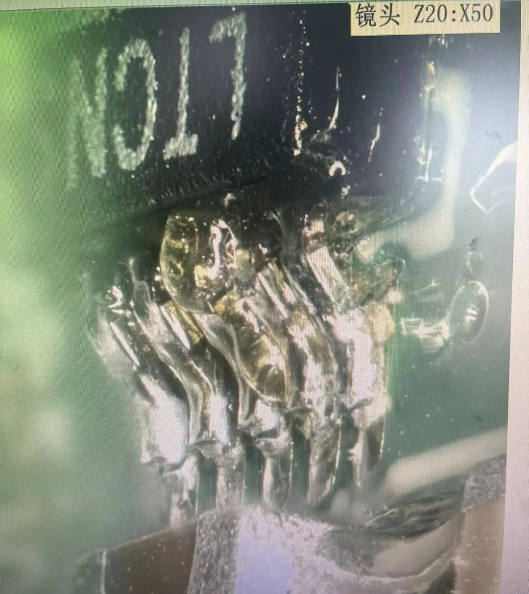
Shuai Shuai: Then half of the IC was glued again, and then the glue was removed, and the IC fell off the circuit board directly. The picture below is the IC that fell off the faulty part
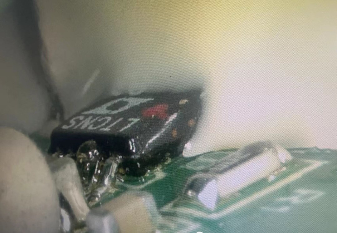
Shuai Shuai: The following pictures are the state of the soldering points on the circuit board after the faulty IC fell off
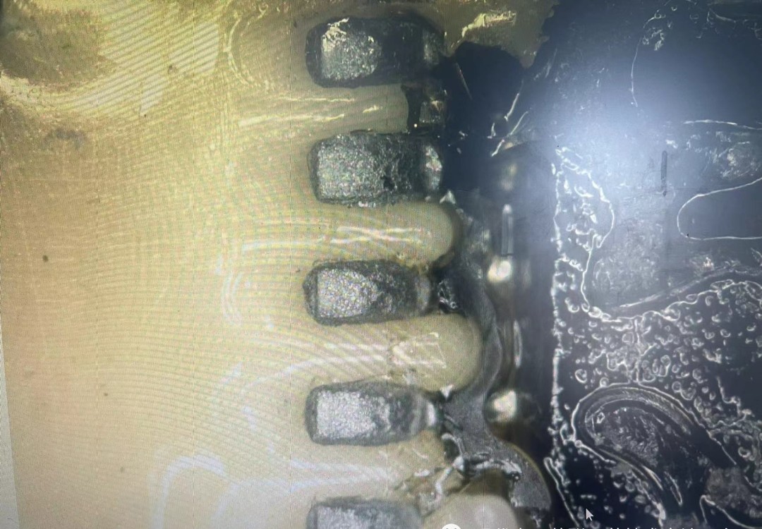
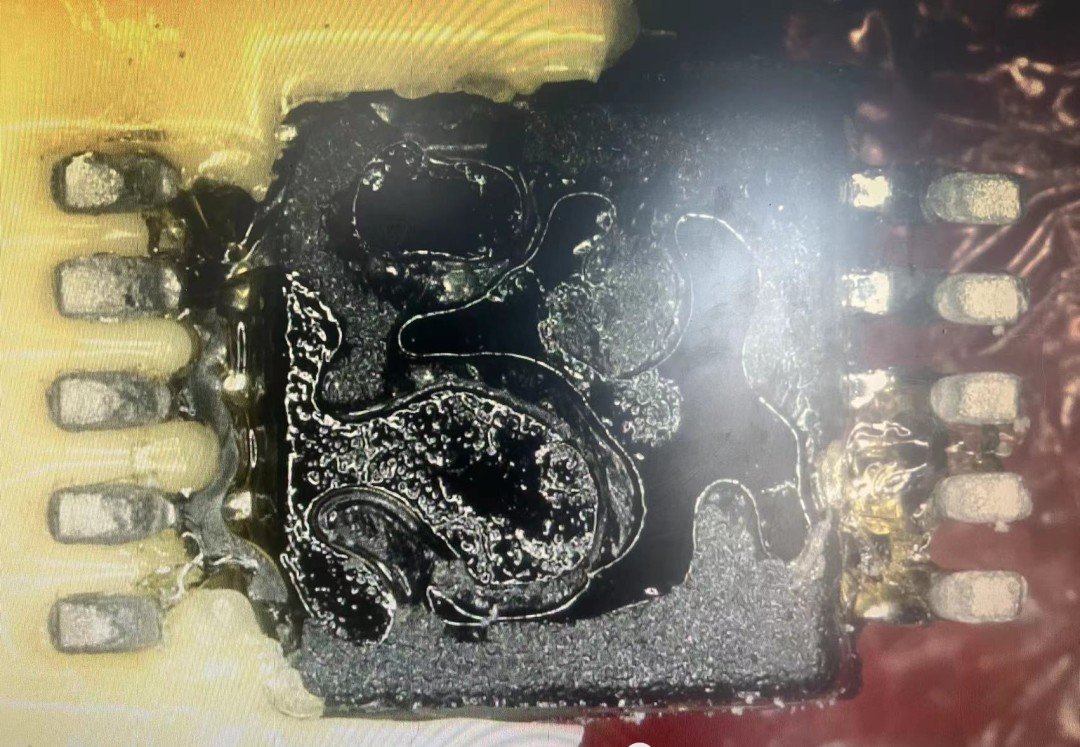
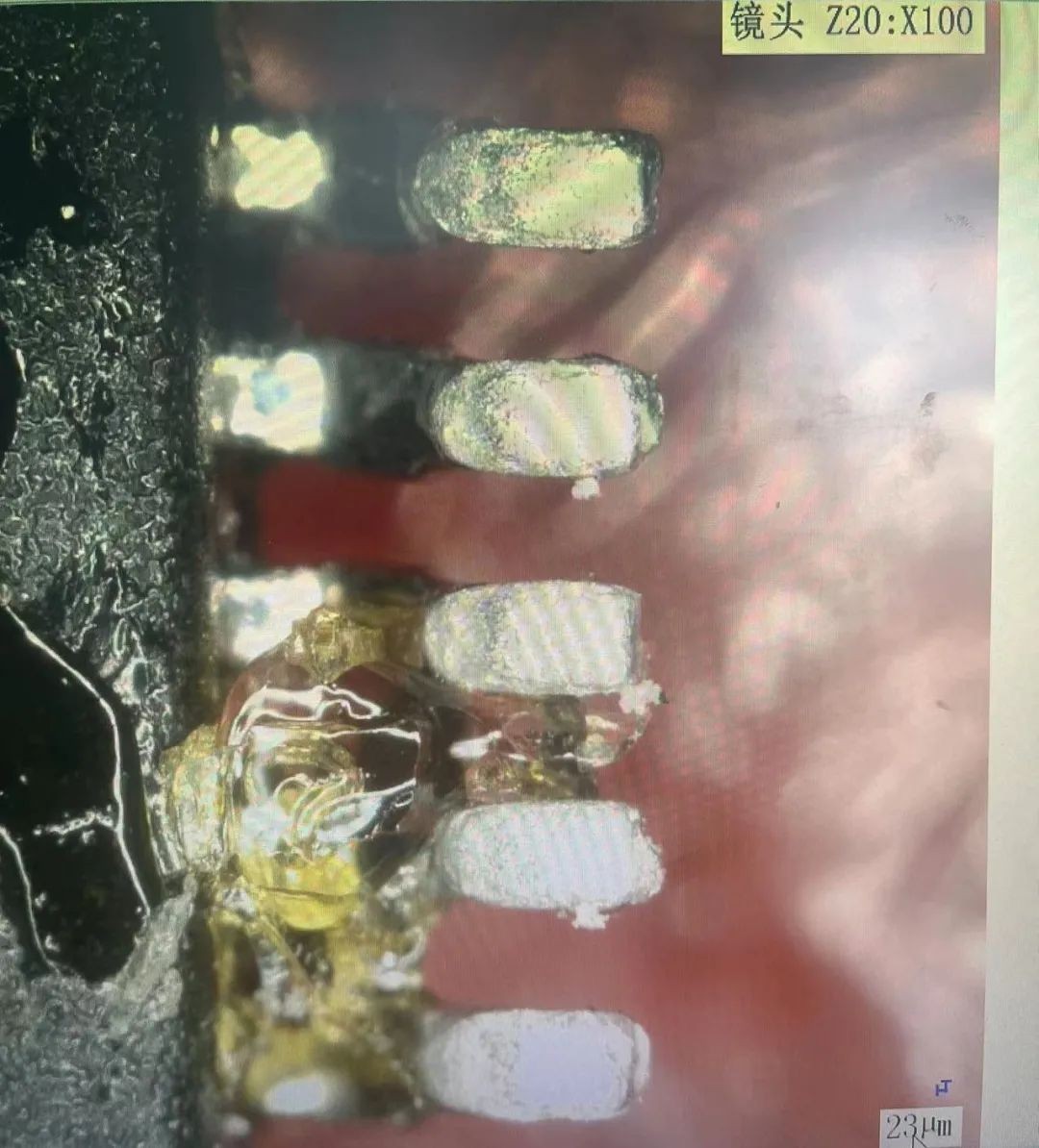
Fish Head: Are other components that have not fallen off also coated with silicone rubber? Is silicone rubber a heat-conductive type? What are the ingredients of silicone rubber, and will there be any reaction between it and the solder joint?
Shuai Shuai: This is the adjacent capacitor welding end, and the others are all attached
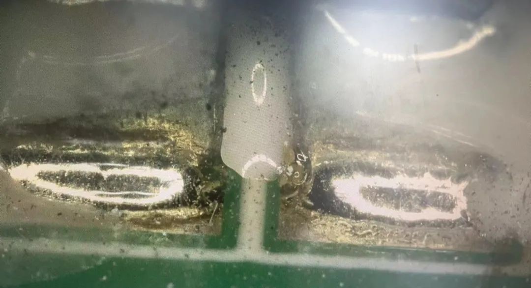
Tyrant: In fact, in this picture, you can see the solder at the heel of the wing-shaped pin formed after the welding is completed, and they are intact on the PCB pad
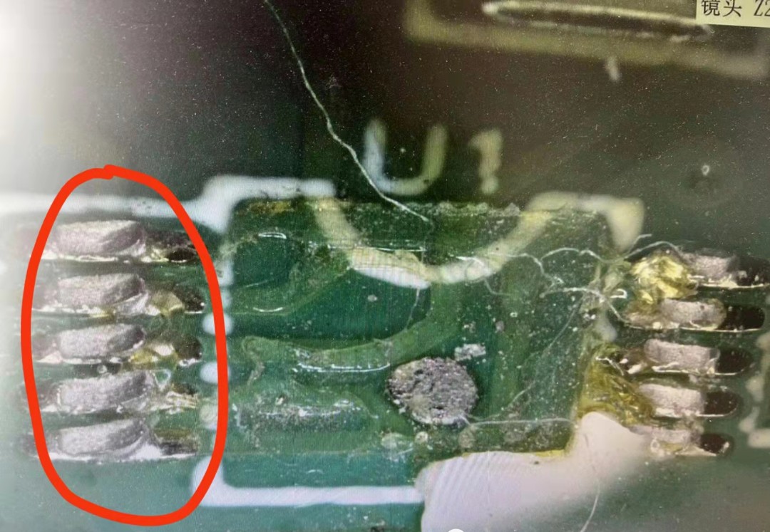
Shuai Shuai: Yes
Tyrant: That is to say, the IMC position connected to the pad may be fine, but the IMC connected to the pin may be defective. Then there is a problem with pin oxidation or pin plating.
Shuai Shuai: Is it possible that the soldering temperature is not high enough?
Tyrant: Let’s ask the manufacturer what the IC pin coating is? Are all other soldering problems OK?
W: Can we see if the device pins are tinned? Eliminate the pin problem
Tyrant: This is not a big heat-generating device
Shuai Shuai: But there is a MOS tube right behind the circuit board. Will it have any impact? And what about the rosin? At the same time, an important information, it is correct to use manual soldering later, and the soldering is good.
Tyrant: Flux residue
Fish head: If there is a problem with the pin oxidation (or coating), can the toe and left and right sides of the pin be wetted to form tin crawling?
Tyrant: I suspect that the workers found that there was a problem with this thing after soldering when they were operating it, and then they added flux, manually soldered it again, etc., and did not clean it properly, so there was a lot of rosin residue left
Shuai Shuai: But later we manually soldered the faulty part, and the soldering was good and the function was normal. The reason for the failure of the faulty parts in the early stage was that there was no output when powered on, and then the abnormal IC solder joints were located.
Tyrant: You can ask the assembly master if they found any abnormalities when soldering this IC.
An Zhinuoran: Take this for analysis and check the IMC composition.
Shuai Shuai: The faulty parts have been damaged.
Tyrant: If the oxidation is not serious, it can still be soldered later.
An Zhinuoran: In theory, the more solder, the higher the reliability. If the soldering time is too long, the IMC composition changes, which can also cause solder joint brittleness.
Tyrant: Let's ask about the pin plating and on-site operation first. If there are stocks in the warehouse, take some to try the solderability.
An Zhinuoran: You can take a few pieces to reproduce the fault and find out the root problem.
Shuai Shuai: At present, it is said that the soldering is poor, and no specific analysis is done later.
Fish Head: The photo of the PCB pads seems a bit strange to me. It seems that the 5 pads on the left are fully wetted (the inner PCB pads of the upper left 2 IC pins still have exposed gold), and the 5 pads on the right, the outer side of the IC is not fully wetted (there is still exposed gold).
In a way, the matching degree of IC lead size, pad design size, and steel mesh opening size is not very good, and the mounting positioning is also biased to one side (the left side in the picture), and there are a lot of rosin residues. Looking back at the faulty products, the overall feeling is that the assembly quality of the IC is not ideal, and QC should intercept it and then release it (after process judgment or review).
How long has the product been installed? What is the ambient temperature and humidity? Is the silicone rubber an addition-type two-component?
Shuai Shuai: Is it possible that the solder joints were not like this at the beginning? I think they have all been specially inspected. With such a welding effect, there are still so many flux residues that cannot flow out
Fish Head: Looking at the picture above, I found that your picture is digitally magnified (the kind of microscope with lens + LCD screen), not optically magnified (stereoscopic microscope, etc.). I always feel that the clarity is not enough and some details are not clear.
Shuai Shuai: They exposed no output during the power-on process
Fish Head: The customer's IQC process found abnormalities? It has not been officially installed and used? You opened the faulty product. Is the silicone rubber completely cured?
Shuai Shuai: It was installed, and it was cured. Because of the weight limit, there was not much glue.
Yutou: Looking at the pictures, there is no sign of secondary welding (re-welding) on the solder joints. After manual re-welding, the exposed gold part of the original PCB pad should have been tinned.
Shuai Shuai: Is there a current too large when the power is turned on, causing secondary melting?
Yutou: It doesn't seem like it. For such a small package, the normal working current of the IC circuit is unlikely to be small. Abnormal overcurrent and overload will most likely burn the PCB circuit or IC, and it is unlikely that it is just a secondary melting of the solder joints.
For products produced in the same batch, it is recommended to use a stereo microscope to carefully observe the solder joints. See if it is a problem with this individual unit or a problem with the (IC abnormality) batch.
Shuai Shuai: Yes, thank you for your help in analyzing, we will discuss it internally!

