The golden rule of switching mode power supply board layout
Optimising the board layout is an important direction when designing switch-mode power supplies. A proper layout ensures that the switching regulator remains stable and that radiated and conducted interference (EMI) is kept as low as possible. This is something that electronics developers are well aware of. However, people do not know what an optimised board layout for a switched-mode power supply should look like.
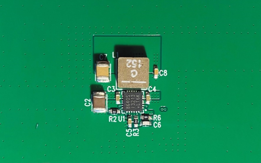
Figure 1 shows the LT8640S evaluation board circuit. It is a step-down switching regulator that supports input voltages of up to 42 V and can provide output currents of up to 6A. All components are arranged closely together. It is generally recommended to arrange the components as closely as possible on the board. There is nothing wrong with this statement, however, it may not be appropriate if the goal is to obtain an optimised board layout. In Figure 1, for example, the switching regulator IC is surrounded by several (11) passive components.
When deploying these passive components, which ones should be given priority? Why?
The most important principle in switching regulator PCB design is that the shorter the alignment for transmitting high switching currents, the better. If this principle can be successfully practised, a large part of the switching regulator board can be reasonably laid out.

How can this golden rule be easily implemented in the layout of a circuit board? The first step is to identify the critical paths in the switching regulator topology. In these critical paths, the current varies in response to switching. Figure 2 shows a typical circuit for a buck converter (buck topology). The critical paths are shown in red. These connection lines may or may not transmit full current, depending on the state of the power switch. The shorter these paths are, the better. In a buck converter, the input capacitor should be as close as possible to the VIN pin and GND pin of the switching regulator IC.

Figure 3 shows the basic schematic of a step-up topology circuit. The circuit converts low voltage to a higher voltage. Again, the current path where the current changes in response to the switching of the power supply is shown in red. It is important to note that the placement of the input capacitors is not at all important. It is the placement of the output capacitor that is more critical. It must be as close as possible to the flyback diode (or high-side switch) and to the ground connection of the low-side switch.
Other arbitrary switching regulator topologies can then be examined to see how the current changes when switching the power supply on and off. The traditional method is generally to print out the circuit and then draw the current path with three different coloured coloured pens. The first colour is used to mark the current path during conduction, i.e., when the power switch is on. The second colour is used to mark the current path during the off period, i.e. when the power switch is switched off. Finally, a third colour is used to mark all the current paths that have previously been marked only in the first colour and only in the second colour. In this way, the critical paths where the current changes with the switching of the power switch can be clearly seen.
The core rule, according to KEY, is to design the paths where the current changes with switching as short and compact as possible. This is simple to explain, fits logically, and is the basis for achieving an optimal board layout in switching mode power supply design.


