Description
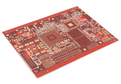
PCB Blind via vs microvia
"microvia" The common interpretations are "micro via; micro via hole; micro through hole". In the field of PCB (Printed Circuit Board), it usually refers to a via hole with a smaller diameter.
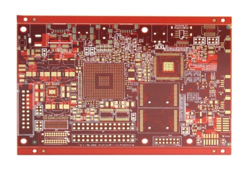
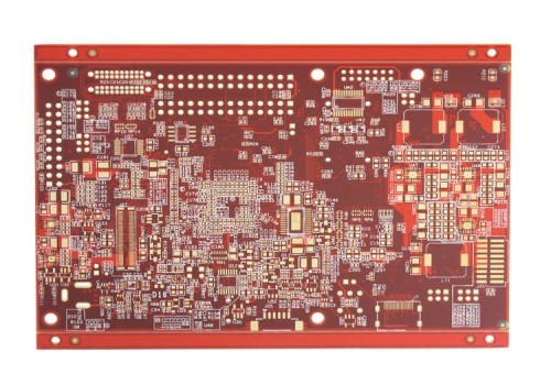
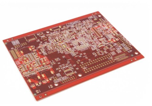
A blind via hole refers to a hole that connects the inner layers of a printed circuit board (PCB) but does not penetrate the entire board. It has an opening on the surface of the PCB at one end and terminates at a certain layer inside the PCB at the other end. Unlike a through hole, it does not completely pass through the entire PCB. Blind via holes are often used in multilayer PCB designs to achieve electrical connections between different inner layers and help increase the wiring density of the PCB and reduce the size of the board.
Microvias can be classified based on several factors:
1. Microvias is classified by size: They can be categorized as small microvias (less than 100 microns in diameter), medium microvias (100 - 150 microns), and large microvias (greater than 150 microns).
2. Microvias is classified by structure: This includes stacked microvias, where multiple microvias are placed one on top of the other, and staggered microvias, where they are arranged in a non-linear pattern.
3. Microvias is classified by material: They can be classified based on the material used for filling the via, such as copper-filled microvias or resin-filled microvias.
4. Microvias is classified by application: Depending on the specific PCB application, they can be classified as microvias for high-speed digital circuits, RF (Radio Frequency) circuits, or power circuits.
5. Microvias is classified by manufacturing process: This could include laser-drilled microvias, mechanical-drilled microvias, or chemically-etched microvias.
A PCB blind via and a microvia are similar in that they both connect inner layers of a PCB without going through the entire board. However, there are some differences:
A blind via is generally larger in size and is often used to connect two or a few specific inner layers of the PCB.
A microvia, on the other hand, is extremely small in diameter, often in the range of a few hundred microns or less. It is used in high-density PCB designs where space is at a premium and a large number of connections need to be made within a limited area.
In summary, the main differences lie in their size and the level of PCB density and complexity where they are typically employed.
The manufacturing processes of blind via holes and microvias have several differences.
For blind via holes, mechanical drilling is commonly used. This involves using a drill bit to create the hole. The diameter of the drill bit is relatively larger compared to that used for microvias.
In contrast, microvias are often fabricated using laser drilling or photoimaging techniques. Laser drilling is precise and can create very small via holes with high accuracy. Photoimaging processes involve applying a photosensitive material and exposing it to light to define the via pattern.
Another difference is in the plating process. Blind via holes usually require thicker plating layers to ensure good conductivity. Microvias, due to their smaller size, may need more advanced plating techniques to achieve uniform coverage and reliable electrical connection.
Furthermore, the inspection and quality control methods for blind via holes and microvias can also vary. Microvias demand more sophisticated inspection equipment and techniques to detect any defects or imperfections given their smaller dimensions.
What are the advantages and disadvantages of blind via holes and microvias respectively?
The advantages of blind via holes include:
1. Blind via holes can provide electrical connections between specific inner layers of the PCB, allowing for better layer management.
2. Blind via holes are relatively easier to manufacture compared to microvias in some cases.
The disadvantages of blind via holes are:
1. They take up more space on the PCB, which may limit the density of components and routing.
2. They may have higher impedance compared to microvias, affecting signal integrity in high-frequency applications.
The advantages of microvias include:
1. Microvias enable higher component density on the PCB, allowing for more complex and compact designs.
2. Microvias offer better signal integrity, especially at high frequencies.
The disadvantages of microvias are:
1. Microvias are more challenging and costly to manufacture, requiring advanced equipment and processes.
2. Microvias have lower current-carrying capacity compared to larger blind holes.
How does the cost comparison of blind via holes and microvias look like?
In general, microvias tend to be more costly than blind via holes.
The manufacturing process of microvias is often more complex and requires more advanced equipment and techniques. They usually involve processes like laser drilling or special plating methods, which increase the production cost.
Blind via holes, on the other hand, can often be produced using more conventional drilling methods and standard plating processes, which are relatively less expensive.
However, the actual cost can also be influenced by factors such as the volume of production, the specific requirements of the PCB design, and the capabilities of the manufacturing facility. In some cases, if there is a high volume production and optimized manufacturing setup for microvias, the cost difference might not be as significant.
What methods can be used to reduce the manufacturing costs of blind via holes and microvias?
The following methods can potentially help reduce the manufacturing costs of blind via holes and microvias:
1. Optimize the PCB design: Minimize the number of blind via holes and microvias required by improving the circuit layout and routing strategies.
2. Improve manufacturing processes: Streamline and optimize the drilling, plating, and other production processes to increase efficiency and reduce waste.
3. Bulk production: Producing a large quantity of PCBs with the same blind via hole and microvia requirements can often lead to economies of scale and lower unit costs.
4. Select appropriate materials: Choosing cost-effective materials for the blind via hole PCB substrate and plating without sacrificing quality and performance.
5. Invest in advanced equipment: While this may involve an upfront cost, modern and efficient manufacturing equipment can improve productivity and reduce long-term costs.
6. Employee training: Well-trained workers can operate the equipment more proficiently, reducing errors and rework, thereby lowering costs.
7. Work with experienced microvias PCB manufacturers: They can offer cost-effective solutions based on their expertise and established supply chains.
