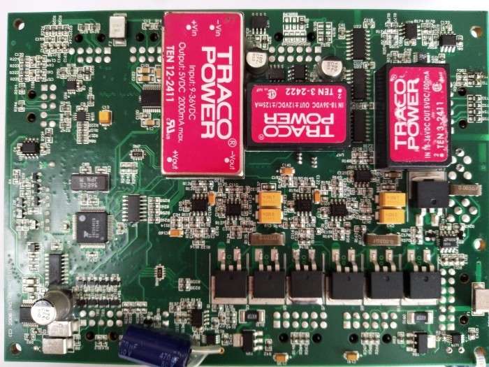
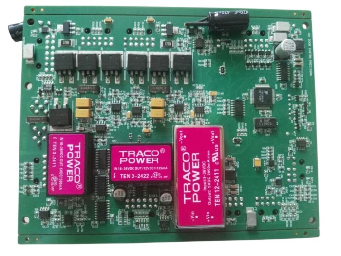
Description
reverse gerber BOM schematic,
reverse program,
reverse IC,
reverse program,copy IC, IC decipher,copy board,
copy gerber,copy bom,copy schematic

PCB reverse engineering, also known as reverse engineering, refers to the analysis and research of the existing PCB to understand its design, structure and function. The following are some common steps and methods of PCB reverse engineering:
1. Clearly define the analysis project: Determine the characteristics of the PCB to be studied, such as line width and spacing, aperture size, copper thickness, etc.
2. Use appropriate analysis instruments: Select the appropriate instruments according to the needs, such as 3D X-RAY, EDS, SEM analyzer, etc.
3. Conduct external observation: Measure and record the external features of the PCB, such as the color of the ink, the size of the PAD, the amount of solder mask offset, etc.
4. Make cross-section analysis: Through cross-section analysis to measure internal characteristics such as copper thickness, hole wall roughness, nail head, etc.
5. Data recording and analysis: Record and analyze the measured data, and compare the product differences of different manufacturers.
6. Combine with the process flow: Combine the analysis results with the process flow and control points of the PCB, and put forward optimization suggestions.
It should be noted that when conducting PCB reverse engineering, it is necessary to follow laws, regulations and ethical norms, and not to infringe on the intellectual property rights of others. At the same time, the results of reverse engineering may have certain errors and need further verification and confirmation.


