Description
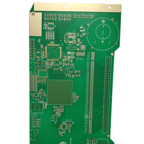
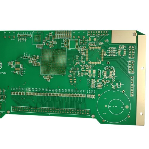
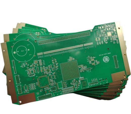
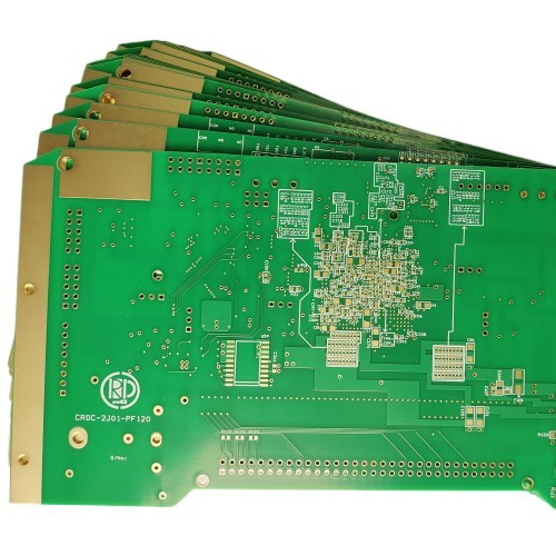
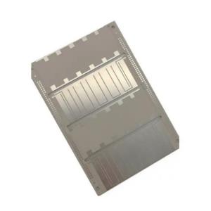
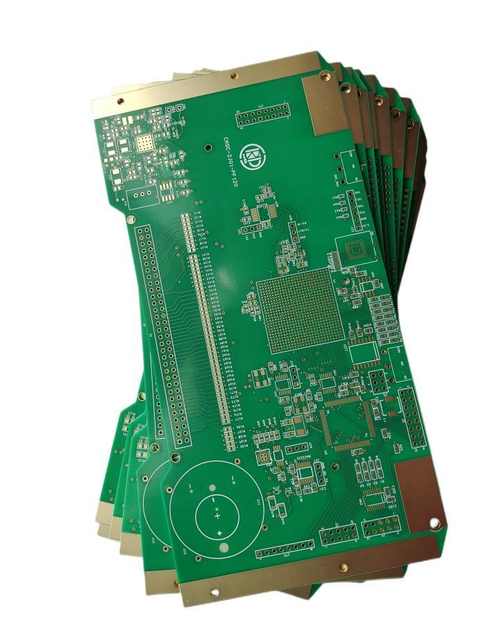
This is rigid PCB, material is FR-4 with green soldermask, surface treatment ENIG (immersion gold) , high TG 170, IPC class III,1oz copper thick, 1.6mm board thick
FR-4 PCB Manufacturing process
The entire process of PCB (Printed Circuit Board) manufacturing typically includes the following steps:
FR-4 PCB Manufacturing process I. PCB design
Engineers use professional PCB design software to create the layout of the circuit board, including the placement of components and the planning of connection lines. How is a PCB (Printed Circuit Board) designed?
The design of a PCB (Printed Circuit Board) typically follows the following steps:
1. Planning and requirements analysis:
- Clearly define the functions and performance requirements of the circuit, determine the required number of layers, board thickness, materials, etc.
- Consider factors such as the complexity of the circuit, signal frequency, current load, etc.
2. Schematic design:
- Use circuit design software to draw the circuit schematic, including various electronic components (such as resistors, capacitors, chips, etc.) and their connections.
3. Component placement:
- Based on the schematic, arrange the positions of the components in the PCB design software.
- Consider factors such as signal flow, distribution of heat-generating components, and wiring difficulty to optimize the layout.
4. Routing:
- Connect the pins of each component, following wiring rules such as minimum line width, line spacing, impedance control, etc.
- Special processing is performed on high-speed signal lines to reduce signal reflection and crosstalk.
5. Power and ground planning:
- Reasonably plan the power layer and ground layer to ensure stable power supply and reduce ground noise.
6. Design rule check (DRC):
- The software automatically checks whether the design complies with the set rules, such as spacing, short circuits, open circuits, and other errors.
7. Signal integrity analysis (SI) and electromagnetic compatibility (EMC) analysis:
- Evaluate the quality, timing, and electromagnetic interference of the signals. If there are problems, optimize them.
8. Generate manufacturing files:
- Generate the files required for PCB manufacturing, such as drilling files, photoplotting files, etc.
PCB design requires comprehensive consideration of multiple factors such as circuit performance, manufacturing processes, and costs. Mastering professional design software and related knowledge proficiently is the key to successful design.
FR-4 PCB Manufacturing process II. Material Preparation
Prepare the raw materials required for making the PCB: FR-4. What material is FR-4?FR-4 is a type of glass fiber-reinforced epoxy-based composite material.It has good electrical properties, mechanical properties, and chemical corrosion resistance. It is often used in the manufacture of printed circuit boards (PCBs). FR-4 material is widely used in the electronics industry because it can provide reliable insulation performance and structural support, and at the same time can withstand various processing techniques in the PCB manufacturing process, such as copper-clad laminates, copper foil, photosensitive films, etchants, etc.
FR-4 PCB Manufacturing process III. Blanking (CUT)
Blanking is the process of cutting the original copper-clad laminate into boards that can be fabricated on the production line. First, understand several concepts:
- UNIT: UNIT refers to the unit pattern designed by the PCB design engineer.
- SET: SET refers to a whole pattern formed by the engineer combining multiple UNITS for reasons such as improving production efficiency and facilitating production. Commonly known as panelization, it includes unit patterns, process edges, etc.
- PANEL: PANEL refers to a board formed by a PCB manufacturer combining multiple SETs and adding tooling board edges for reasons such as improving efficiency and facilitating production.
FR-4 PCB Manufacturing process IV. Inner Dry Film (INNER DRY FILM)
The inner dry film is the process of transferring the inner layer circuit pattern onto the PCB. This process includes multiple procedures such as inner layer film application, exposure and development, inner layer etching, etc. The specific steps are as follows:
- Pretreatment: The main purpose of grinding the board is to address issues of surface cleanliness and roughness, remove oxidation, increase the roughness of the copper surface, and facilitate the adhesion of the film to the copper surface.
- Film Application: Apply dry or wet film to the treated substrate by hot pressing or coating to facilitate subsequent exposure production.
- Exposure: Align the negative film with the substrate with the applied dry film on the exposure machine, and transfer the pattern of the negative film onto the photosensitive dry film using ultraviolet light.
- Development: Use a weakly alkaline developing solution (sodium carbonate) to dissolve and rinse away the unexposed dry/wet film, while the exposed part remains.
- Etching: The unexposed dry/wet film is removed by the developing solution to expose the copper surface. Use acidic cupric chloride to dissolve and etch away this exposed copper surface to obtain the required circuit.
- Film Stripping: Use a sodium hydroxide solution to remove the exposed dry film that protects the copper surface, revealing the circuit pattern.
FR-4 PCB Manufacturing process V. Browning
The purpose of browning is to form a microscopic roughness and an organic metal layer on the inner copper surface to enhance the adhesion between layers.
FR-4 PCB Manufacturing process VI. Lamination
Lamination is the process of bonding each layer of the circuit into a whole with the help of the adhesiveness of the PP sheet. In practice, materials such as copper foil, adhesive sheets (semi-cured sheets), inner layer boards, stainless steel, spacer plates, kraft paper, and outer steel plates are stacked according to process requirements.
FR-4 PCB Manufacturing process VII. Drilling
How are the holes on the PCB board made?
The holes on the PCB board are mainly made through two methods: mechanical drilling and laser drilling.
Mechanical drilling is the most traditional and fundamental method for PCB drilling. Using a micro drill that rotates at high speed, the holes of the required size are precisely drilled according to the design drawings. Mechanical drilling is suitable for through-hole processing and can handle holes from standard diameters to very small sizes. The drill bit material is usually carbide to ensure processing accuracy and durability. To improve drilling efficiency and accuracy, modern drilling machines are usually equipped with precise positioning systems and automatic tool change devices.
Laser drilling is a non-contact processing method that has been widely used with the development of high-density PCBs. Lasers can quickly and precisely form tiny blind holes or buried holes on PCBs, and are particularly suitable for the production of HDI boards. Laser drilling is divided into several types such as carbon dioxide laser and ultraviolet laser. Compared with mechanical drilling, laser drilling has higher accuracy and flexibility, but the cost is relatively higher.
In practical applications, the choice of which drilling method depends on specific requirements and the characteristics of the PCB.
FR-4 PCB Manufacturing process VIII. Outer Dry Film
Similar to the inner dry film, transfer the outer layer circuit pattern onto the PCB.
When manufacturing a PCB, how is the outer dry film produced? The manufacturing process flow of the outer dry film of PCB usually includes the following steps:
1. Prepare materials: Select the appropriate dry film material, which is usually a photosensitive polymer film.
2. Clean the substrate: Ensure the surface of the PCB substrate is clean, free of oil stains and impurities to ensure good adhesion of the dry film.
3. Apply the film: Attach the dry film to the outer layer of the PCB substrate by means of hot pressing or roller pressing.
4. Exposure: Use a UV light source of a specific wavelength to expose the dry film through a photomask with the circuit pattern. The dry film in the exposed area undergoes a chemical reaction.
5. Development: Put the exposed PCB board into the developer, and the unexposed dry film is dissolved and removed, leaving the required circuit pattern.
6. Etching: Use an etching solution to remove the copper layer that is not protected by the dry film to form the circuit.
7. Stripping the film: Use a stripping agent to remove the remaining dry film to complete the manufacturing of the outer layer circuit.
It should be noted that the specific process flow may vary depending on different manufacturers and product requirements.
FR-4 PCB Manufacturing process IX. Pattern Plating
The specific operation of pattern plating for circuit boards is the process of plating a thin layer of other metals or alloys on the surface of certain metals using the principle of electrolysis. The specific operation process is as follows:
1. Board feeding: Put the PCB board into the plating equipment.
2. Degreasing: Use degreasing agent to remove grease and contaminants on the surface of the PCB board to ensure the adhesion of the plating layer.
3. Water washing: Rinse the PCB board with water to remove residual degreasing agent and contaminants.
4. Microetching: Use microetching agent to slightly etch the surface of the PCB board to increase the adhesion of the plating layer.
5. Water washing: Rinse the PCB board with water to remove the residual microetching agent.
6. Acid dipping: Immerse the PCB board in acid solution to remove oxides and impurities on the surface.
7. Copper plating: Plate a layer of copper on the PCB board to increase the conductivity and wear resistance of the circuit.
8. Water washing: Rinse the PCB board with water to remove the residual plating solution.
9. Acid dipping: Immerse the PCB board in acid solution to remove oxides and impurities on the surface.
10. Plating lead-tin: Plate a layer of lead-tin on the PCB board to protect the circuit and improve the soldering performance.
11. Water washing: Rinse the PCB board with water to remove the residual plating solution.
12. Board discharging: Take the plated PCB board out of the plating equipment.
13. Strip plating: Use stripping solution to remove the unnecessary plating layer on the PCB board.
14. Water washing: Rinse the PCB board with water to remove the residual stripping solution.
15. Board feeding: Put the PCB board into the next process.
During the pattern plating process, parameters such as plating time, current density, and solution temperature need to be controlled to ensure the plating quality. At the same time, attention should also be paid to environmental protection issues during the plating process, and appropriate wastewater treatment measures should be taken.
FR-4 PCB Manufacturing process X. Etching
The etching process in the PCB (Printed Circuit Board) manufacturing process is to remove the unnecessary copper foil on the circuit board through chemical corrosion to obtain the required circuit pattern. The specific steps are as follows:
1. Film stripping: Use the film stripping solution to remove the exposed dry film on the board, exposing the copper foil that needs to be etched.
2. Etching: Put the board into the etching tank, and the etching solution will have a chemical reaction with the copper foil to corrode the exposed copper foil. The type and concentration of the etching solution will affect the etching speed and effect.
3. Tin stripping: Use the tin stripping solution to dissolve the tin layer left on the board after etching to restore the original color of copper to the circuit.
During the etching process, the following points need to be noted:
1. Selection of etching solution: Select the appropriate etching solution according to different circuit board types and etching requirements. Common etching solutions include acidic etching solution and alkaline etching solution.
2. Etching time and temperature: Control the etching time and temperature to ensure the etching depth and uniformity.
3. Side etching control: Side etching may occur during the etching process, that is, the etching solution will not only corrode the copper foil but also the surrounding substrate. To reduce side etching, methods such as using the appropriate etching solution, controlling the etching time and temperature, and adding an anti-corrosion layer can be adopted.
4. Environmental protection treatment: Waste liquid and waste gas will be generated during the etching process, and environmental protection treatment is required to reduce environmental pollution.
FR-4 PCB Manufacturing process XI. Solder Mask Printing
The solder mask process during the manufacturing of PCB (Printed Circuit Board) plays a crucial role.
The solder mask process mainly comprises the following steps:
1. Pretreatment: The PCB board undergoes cleaning and micro-roughening to enhance the adhesion of the solder mask layer.
2. Printing of the solder mask ink: The solder mask ink is uniformly applied onto the PCB board through methods such as screen printing or inkjet printing. All areas except those that require soldering (such as pads, vias, etc.) are covered.
3. Pre-baking: The PCB board coated with the solder mask ink is pre-baked to remove the solvents in the ink and achieve initial curing.
4. Exposure: Ultraviolet light is used to pass through a film with a specific pattern to expose the solder mask ink. The solder mask ink in the exposed areas undergoes a chemical reaction, enabling it to be retained during the subsequent development process.
5. Development: The exposed PCB board is placed in the developer, and the unexposed solder mask ink is dissolved and removed, revealing the areas that need soldering.
6. Post-baking: The developed PCB board undergoes high-temperature baking to ensure complete curing of the solder mask ink and form a robust solder mask layer.
The main functions of the solder mask process are:
1. To prevent the circuits on the PCB board from oxidation and corrosion during storage, transportation, and usage.
2. To reduce the risk of short circuits and enhance the reliability of the circuit.
3. To provide insulation protection and prevent signal interference between adjacent lines.
4. To give the PCB board an aesthetically pleasing appearance.
In conclusion, the solder mask process is of great significance for improving the quality and performance of the PCB.
FR-4 PCB Manufacturing process XII. silkscreen
During the PCB (Printed Circuit Board) manufacturing process, silk-screened characters are an important aspect.
Silk-screened characters refer to various identifications, symbols, and textual information printed on the surface of the PCB board through the silk-screen printing method. These characters typically include the names, numbers, polarity marks, version numbers, manufacturer information, etc. of the components.
The main functions of silk-screened characters are as follows:
1. Facilitating assembly and repair: During the PCB assembly process, workers can quickly and accurately identify the position and direction of components through silk-screened characters, improving the assembly efficiency and accuracy. During repairs, faulty components can also be quickly located based on the character identifications.
2. Providing product information: Silk-screened characters can contain information such as the product version, batch, manufacturer, etc., which is helpful for quality control and traceability.
3. Improving readability and comprehensibility: Clear character identifications make it easier for users and technicians to understand the function and layout of the PCB.
The manufacturing process of silk-screened characters usually includes the following steps:
1. Design the character pattern: In the PCB design software, determine the character content, font, size, and position that need to be printed.
2. Make the silk-screen template: According to the designed character pattern, make the corresponding silk-screen template.
3. Prepare the ink: Select the ink suitable for the PCB material and the usage environment.
4. Print the characters: Place the PCB board on the printing equipment and print the ink onto the designated position of the PCB board through the silk-screen template.
5. Cure the ink: After printing, cure the ink through methods such as heating or ultraviolet radiation to ensure the firmness and clarity of the characters.
In conclusion, although silk-screened characters seem simple in PCB manufacturing, they are of great significance for the assembly, repair, and use of the PCB.
FR-4 PCB Manufacturing process XIII. Surface Treatment
In the PCB (Printed Circuit Board) manufacturing process, the common surface treatment methods and their practices are as follows:
1. Hot Air Solder Leveling (HASL): Firstly, immerse the PCB in molten tin-lead alloy, and then use hot air to level it, ensuring that the tin-lead evenly covers the solder pads of the PCB. This method has a relatively low cost but may have issues with flatness and coplanarity.
2. Organic Solderability Preservative (OSP): Immerse the PCB in a solution containing special organic substances. These organic substances form a protective film on the copper surface to prevent oxidation and can be removed by the flux during soldering, exposing the clean copper surface for soldering.
3. Electroplated Nickel Gold: First, electroplate a layer of nickel on the PCB surface, and then a thin layer of gold. Nickel provides good corrosion resistance and wear resistance, while gold has excellent electrical conductivity and solderability.
4. Electroless Nickel Immersion Gold (ENIG): Deposit a layer of nickel-phosphorus alloy on the PCB surface through a chemical reaction, and then deposit a layer of gold.
5. Immersion Silver: Deposit a layer of silver on the PCB surface using a chemical method. It has good electrical conductivity and solderability, but the silver layer is prone to oxidation.
Different surface treatment methods have their own advantages and disadvantages. The choice of which method to use depends on factors such as the application requirements of the PCB, cost, and reliability requirements.
FR-4 PCB Manufacturing process XIV. Final Inspection
How is the final inspection carried out in the PCB manufacturing process? In the process of PCB (Printed Circuit Board) manufacturing, the final inspection usually includes the following aspects:
1. Appearance inspection: Check whether the surface of the PCB has scratches, stains, discoloration, blisters and other defects. At the same time, confirm whether the solder mask layer is uniform and complete, and whether the character markings are clear and accurate.
2. Circuit inspection: Use optical inspection equipment or microscopes to carefully check whether the integrity, width, and spacing of the circuits meet the design requirements, and whether there are problems such as open circuits, short circuits, and notches.
3. Hole position inspection: Check whether the drilling positions and hole diameters on the PCB are accurate, and whether there are impurities in the holes and whether the plating layer is complete.
4. Electrical test: Use professional testing instruments to test parameters such as resistance, capacitance, and inductance of the PCB to ensure that the electrical performance of the circuit meets the requirements. Conductivity tests will also be carried out to check whether the lines are conducting normally.
5. Solderability test: Sample the solder pads of the PCB for solderability tests to ensure that solder can adhere well during subsequent soldering processes.
6. Dimension measurement: Measure the length, width, thickness and other dimensions of the PCB to confirm whether they meet the design specifications.
7. Packaging inspection: Check whether the packaging of the PCB can effectively protect the board from damage during transportation and storage, and whether the packaging markings are clear and accurate.
The purpose of the final inspection is to ensure that the quality of the PCB meets relevant standards and the requirements of customers. Only PCB products that pass the final inspection can be delivered for use.
