How are stamped hole packages made in PCB design?
[Read More] Stamp hole: inside the main board assembly, small plates and small plates need to be connected between the tendons, in order to facilitate cutting, the tendons above will open some small holes, similar to the edge of the stamp kind of hole. Shaped like a postage stamp in the division of the round hole design, the advantages of its strength than V-Cut good, can be directly broken, but the disadvantage is that the folding surface is not easy to control the precise, if the distance from the line too, easy to appear line damage, instead of causing scrap.
4.26 PCB design in the stamp hole package how to make?
A: Stamp holes: inside the motherboard assembly, small boards and small boards need to be connected between the tendons, in order to facilitate the cutting, the tendons will be opened above some small holes, similar to the edge of the kind of postage stamps holes. Shaped like a stamp in the division of the round hole design, the advantage of its strength than V-Cut good, can be directly broken, but the disadvantage is that the fracture surface is not easy to control the precise, if the distance from the line is too, easy to appear line damage, instead of causing scrap.
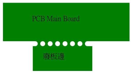
Figure 4-64 Stamped hole splicing board
Generally speaking, PCB splicing can be used stamp hole technology or double-sided engraved V-slot partitioning technology, in the use of stamp holes, attention should be paid to the edge of the lap should be evenly distributed around each splicing board to avoid welding due to uneven forces on the PCB board and lead to deformation.
Notes for adding stamp holes.
1) Spacing between the pieced board and the board 1.6mm to 2mm etc.
2) Stamp holes: 8-10 holes of 0.5mm, hole spacing:0.2mm, hole centre distance:1mm.
(3) Add two rows, stamp holes extend into the board, if the board edge is wired to avoid (Extend into the board: the burr left after breaking does not affect the external dimensions. We often say with negative tolerances). After adding the stamp hole, the shape of the two sides of the hole are connected to facilitate the continuation of the gong with the system after the work.
Steps for the production of stamp holes.
(1) the implementation of the menu command "Place → Pad" to place the 0.5mm pad to the board frame line, the stamp hole is non-metallised without disk hole, so the hole and disk size are 0.5mm, as shown in Figure 4-65, uncheck the "Plated" that is a non-metallised hole.
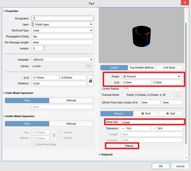
Figure 4-65 Stamp hole property settings
(1) Copy the holes, use "Special Paste" to copy and paste the pads directly in the original place, with a centre spacing of 1mm, copy the number of 4-5, and place them on the two sides of the plate frame, as shown in Figure 4-66.
(2) the implementation of the menu command "Placement → arc → arc (edge)" can also be implemented Altium shortcut key "PAE" quickly placed arc, the command position as shown in Figure 4-67. And click on the upper and lower two over the hole to connect the two sides of the shape of the hole, so that our stamp hole production is complete, the effect of the completion of the figure shown in Figure 4-68.
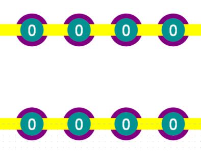
Figure 4-66 Hole placement diagram
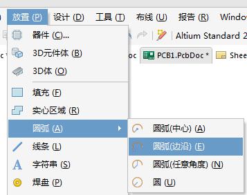
Figure 4-67 Placing the arcs
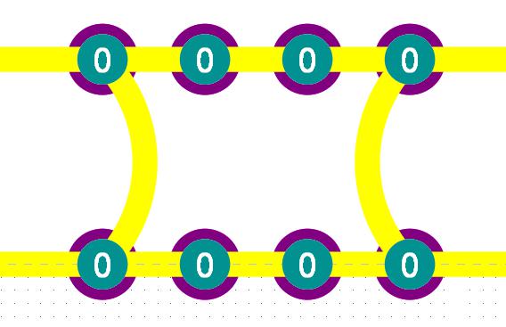
Fig. 4-68 Stamp hole pieced plate
