FR-4 PCB manufacturing process-Solder Mask Printing
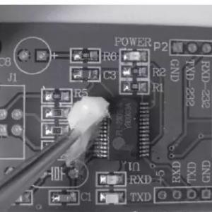
In the manufacturing process of PCB (Printed Circuit Board), the solder mask process is an important stage.The main function of the FR-4 PCB manufacturing solder mask layer is to prevent the areas that do not require soldering from being mistakenly soldered during the subsequent assembly process and to protect the circuit lines on the surface of the circuit board from erosion by the external environment, such as dust, moisture, and chemical substances, thereby enhancing the reliability and service life of the circuit board.
The FR-4 PCB manufacturing process solder mask printing typically includes the following main steps:
First is the preparatory work, which requires ensuring that the surface of the PCB is clean, free of grease, and impurities.
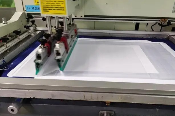
Then, through the method of silk-screen printing, the solder mask ink is evenly applied onto the PCB. The silk screen is usually fabricated based on the design pattern of the PCB, with only the areas corresponding to the solder pads and vias that need to be exposed being hollowed out.

After the FR-4 PCB manufacturing process solder mask printing is completed, the solder mask ink is pre-baked to remove some solvents and achieve initial curing.
Next is the exposure step. Using a specific exposure device and mask, ultraviolet light or other light sources are shone onto the solder mask layer. The parts exposed to the light undergo a chemical reaction, thereby changing their solubility.
After FR-4 PCB manufacturing process solder mask printing exposure, the PCB undergoes the development process to remove the solder mask ink in the unexposed areas, exposing the solder pads, vias, and other areas that require soldering.
After the development is completed, the solder mask layer undergoes final curing treatment, usually through high-temperature baking, to fully cure the solder mask layer and achieve good physical and chemical properties.
Throughout the entire FR-4 PCB manufacturing solder mask printing process, parameters such as the thickness of the ink, the precision of printing, the energy and time of exposure, the conditions of development, and the temperature and time of curing need to be strictly controlled to ensure that the quality and performance of the solder mask layer meet the design requirements.
In the solder mask printing process of PCB manufacturing, each step has a specific and crucial role:
1. FR-4 PCB manufacturing process solder mask printing-preparation work:
- Cleaning the PCB surface: Removing grease, dust, and impurities to ensure that the solder mask ink can adhere well to the PCB. If the surface is not clean, it may cause problems such as voids, blisters, or detachment of the solder mask layer, affecting the solder mask effect and reliability.
2. soldermask printing:
- Uniformly applying the solder mask ink: Through the hollowed-out parts of the silk screen, the solder mask ink is accurately printed onto the designated areas of the PCB. This step ensures the initial coverage of the solder mask layer and lays the foundation for subsequent processing. Uniform coating helps to ensure the consistency of the thickness of the solder mask layer and avoid local areas that are too thin or too thick.
3.FR-4 PCB manufacturing process solder mask printing-pre-baking:
- Removing some solvents: Enabling the initial curing of the solder mask ink and increasing its viscosity and stability. This helps maintain the shape and position of the solder mask layer during subsequent operations and prevent the ink from flowing and deforming.
4. FR-4 PCB manufacturing process solder mask printing exposure:
- Initiating a chemical reaction: Through the irradiation of a specific light source, the solder mask ink in the exposed parts undergoes a chemical change to alter its solubility. The exposed solder mask ink can resist the erosion of the developer in the subsequent development process, thereby forming an accurate solder mask pattern.
5. FR-4 PCB manufacturing process solder mask printing-development:
- Removing the solder mask ink in the unexposed parts: Exposing the solder pads, vias, and other areas that require soldering. The accuracy of development directly affects the alignment accuracy of the solder mask layer with the solder pads and vias, as well as the soldering quality during the final PCB assembly.
6. FR-4 PCB manufacturing process solder mask printing-curing:
- Fully curing the solder mask layer: Through high-temperature baking, the physical and chemical properties of the solder mask layer are fully enhanced, such as hardness, corrosion resistance, heat resistance, etc. The fully cured solder mask layer can better protect the PCB lines and improve the stability and reliability of the PCB under various environmental conditions.
In summary, each step in the FR-4 PCB manufacturing older mask process is interrelated and indispensable, working together to form a high-quality and reliable solder mask layer, thereby ensuring the normal function and long-term stability of the PCB.


