Description
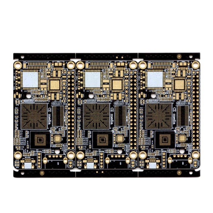
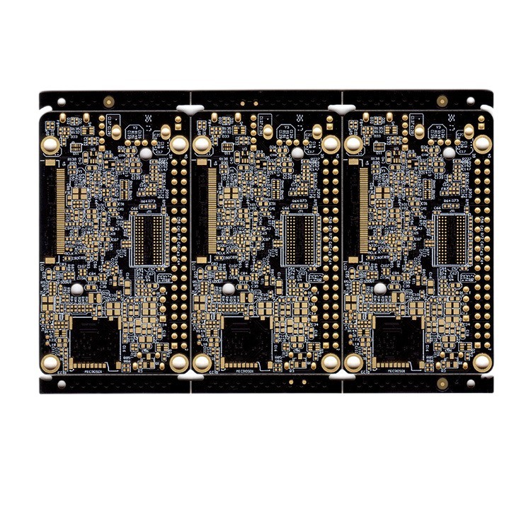
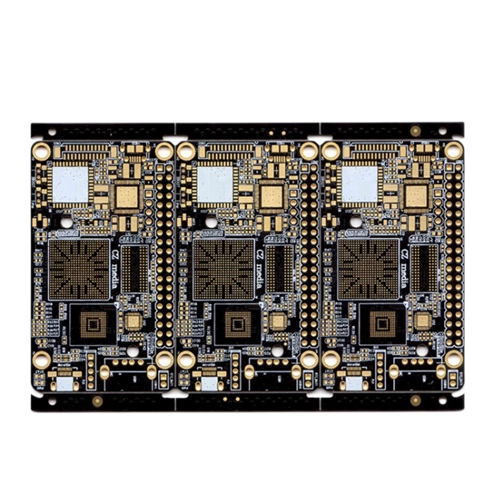
6 layer 2step HDI high-precision buried blind hole HDI PCB
2step HDI 6LAYER PCB,
PCB board thick 1.6 mm,
Plate used FR4 ShengYi,
Minimum hole diameter 0.1mm,
Surface treatment ENIG,
BGA size 0.25mm,
Minimum trace width/distance 0.13mm/0.15mm,
Blind hole structure 6 layer 2step HDI,
Process characteristics HDI blind hole process,
high BGA density, small spacing between hole to trace,
Application field: communication
To improve the reliability of HDI technology in the PCB field, the following aspects can be considered:
- Optimize the design of blind vias: There are voids in the blind vias, and there is remaining air in them, which affects the reliability after thermal shock. The conventional method to solve this problem is to fill the voids in the blind vias with resin or fill the blind vias with resin plugging vias through lamination.
- Select the appropriate PCB materials: Different PCB materials have different adaptabilities to the HDI process, so it is necessary to select the appropriate PCB materials according to the specific application scenario.
- Control the blind via hole shape: The blind via hole shape has an impact on the electroplating filling effect, so it is necessary to control the blind via hole shape to ensure a good filling effect.
- Adopt advanced equipment and processes: Using advanced equipment and processes can improve the reliability and accuracy of HDI technology. For example, using laser drilling can improve the drilling accuracy, and using electroplating to fill the blind vias can improve the reliability of the blind vias.
- Strictly control the production process: In the production process, it is necessary to strictly control the process parameters of each link to ensure the stability and consistency of product quality.
- Conduct reliability tests: Conduct reliability tests on the produced PCB to timely discover and solve potential problems to improve the reliability of the product.


