Description
What is Flexible Printed Circuit (FPC)?
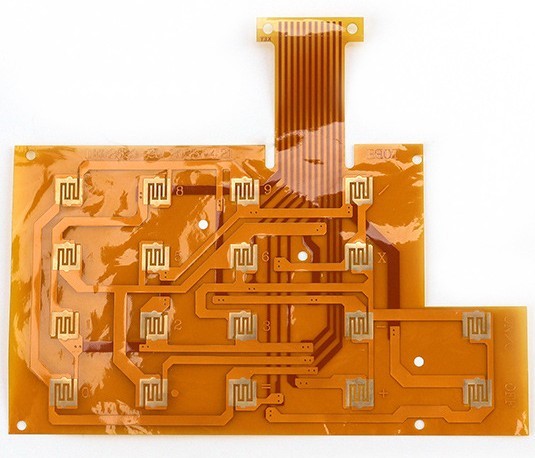
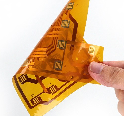
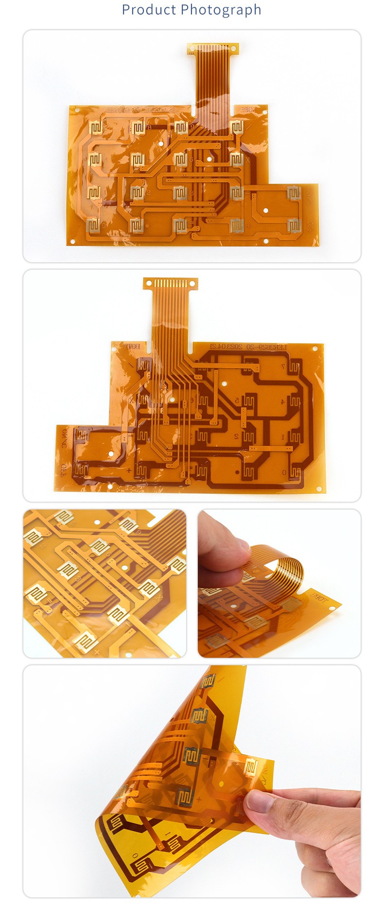
Flexible Printed Circuit (FPC), also known as flexible circuit board or flexible printed wiring board, is a printed circuit board made of polyimide or polyester film as the base material, featuring high reliability and excellent flexibility.
It uses flexible insulating materials as the substrate. Through specific manufacturing processes, conductive circuits, soldering points, and installation areas for various electronic components are formed on it, which can realize the transmission of electronic signals and electrical connections. Compared with traditional rigid printed circuit boards, flexible printed circuit boards are thin, light, bendable, foldable, and can be coiled. They can adapt to various complex spatial layouts and special application scenarios, such as achieving compact internal connections in small electronic devices or providing stable electrical connections in components that require dynamic bending.
How many types of lamination structures are there for flexible printed circuit boards?
There are several main types of lamination structures of flexible printed circuit boards (FPCs) according to the complexity of the design and functional requirements:
1. Single-layer Flexible Printed Circuit Board
- Structure: It only consists of one layer of conductive circuit (copper foil) and one layer of insulating substrate (such as polyimide PI or polyester PET).
- Characteristics: It is the simplest structure, with low cost and thin thickness (usually ≤ 0.1mm).
- Applications: It is suitable for scenarios with low requirements for space and simple signal transmission, such as the connection of mobile phone batteries and the simple circuits of small electronic devices.
2. Double-layer Flexible Printed Circuit Board
- Structure: It contains two layers of conductive circuits, with one layer of insulating substrate sandwiched in the middle, and the upper and lower layers of circuits are connected through vias (metallized holes).
- Characteristics: It supports double-sided wiring, improves the circuit density, and the thickness is about 0.15 - 0.2mm.
- Applications: It is commonly found in devices that require two-way connections, such as camera modules and display cables.
3. Multilayer Flexible Printed Circuit Board
- Structure: It is composed of three or more alternating stacked conductive layers and insulating layers, and the layers are connected by blind vias, buried vias or through vias.
- Characteristics: It has a high degree of integration and can realize complex signal transmission. The thickness is usually between 0.3 - 1.0mm.
- Applications: High-end electronic products (such as foldable mobile phones, drones), automotive electronics (sensors, controllers), etc.
4. Coverlay Layer
- Structure: An insulating film (such as PI or PET) is covered on the surface of the conductive circuit layer to protect the circuit and enhance the environmental resistance.
- Characteristics: It is optional and is commonly used in single-layer or double-layer boards to improve reliability.
- Applications: Scenarios with high requirements for moisture-proof and wear-resistant properties, such as consumer electronics and medical devices.
5. Rigid-Flex Printed Circuit Board
- Structure: A rigid circuit board (with FR4 substrate) is combined with a flexible printed circuit board, and they are fixed mechanically or connected directly.
- Characteristics: It has both the support of the rigid board and the bendability of the flexible board, and is suitable for complex spatial layouts.
- Applications: Motherboards of laptops, aerospace equipment, industrial control modules, etc.
Other Special Structures
- Double-sided Copper-clad Flexible Board: There is copper foil on both sides, supporting double-sided circuit design.
- Multilayer Blind and Buried Via Boards: The density is further increased through blind vias (connecting only the surface layer and inner layers) or buried vias (connection between inner layers).
- Flexible Board with Stiffener Layer: Rigid materials (such as FR4) are added to local areas to enhance the mechanical strength and avoid breakage caused by frequent bending.
Conclusion
The lamination structures of flexible printed circuit boards usually fall into five major categories: single-layer, double-layer, multilayer, coverlay layer, and rigid-flex boards. The specific choice needs to be determined according to the complexity of the application scenario, space limitations, and cost budget. If you need to further discuss the design details or application cases of specific structures, feel free to ask!
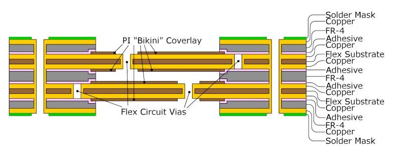
Lamination structure diagrams of flexible printed circuit boards with different layers
The lamination structures of flexible printed circuit boards (FPCs) with different layers can be classified into the following types according to the number of layers and functional requirements. Here are the typical structures and schematic illustrations of different layer numbers:
1. Single-layer Flexible Printed Circuit Board
- Structure:
Substrate layer (PI/PET) → Copper foil layer (conductive circuit) → Coverlay layer (PI/PET)
- Substrate: Polyimide (PI) or polyester (PET), with a thickness of about 0.0125 - 0.1mm.
- Copper foil: Electrolytic copper foil or rolled copper foil, with a thickness of 12 - 35μm.
- Coverlay: Protects the circuit and an open window design can be selected for soldering.
- Characteristics: The thinnest and lightest, with a thickness ≤ 0.1mm and low cost.
- Applications: Mobile phone battery connections, simple circuits of small devices.
2. Double-layer Flexible Printed Circuit Board
- Structure:
Substrate layer (PI/PET) → Copper foil layer (circuit) → Adhesive layer (acrylic/epoxy resin) → Copper foil layer (circuit) → Coverlay layer
- The layers are connected by metallized vias.
- Characteristics: Supports double-sided wiring, with a thickness of about 0.15 - 0.2mm.
- Applications: Camera modules, display cables.
3. Multilayer Flexible Printed Circuit Board
- Structure:
The substrate layer + copper foil layer + adhesive layer are stacked alternately (such as 3 layers, 4 layers, 6 layers, etc.). The layers are connected by blind vias, buried vias or through vias.
- Example (4-layer board):
Substrate → Copper foil (Layer 1) → Adhesive layer → Copper foil (Layer 2) → Substrate → Copper foil (Layer 3) → Adhesive layer → Copper foil (Layer 4) → Coverlay
- Characteristics: High-density integration, with a thickness of 0.3 - 1.0mm, and supports complex signal transmission.
- Applications: Foldable mobile phones, automotive sensors.
4. Rigid-Flex Printed Circuit Board
- Structure:
Rigid layer (FR4 substrate + copper foil) + Flexible layer (PI substrate + copper foil) are connected by mechanical fixation or directly.
- The rigid part provides support, and the flexible part can be bent.
- Characteristics: Combines the properties of rigidity and flexibility, suitable for three-dimensional space layout.
- Applications: Laptop motherboards, aerospace equipment.
5. HDI (High-Density Interconnect) Flexible Board
- Structure:
- Single build-up layer (for example, a 6-layer board): 1 + 4 + 1 structure (surface layer + 4 inner layers + surface layer), laminated once, and blind vias are drilled by laser.
- Double build-up layer (for example, an 8-layer board): 1 + 1 + 4 + 1 + 1 structure, laminated three times, and supports buried vias and cross-layer blind vias.
- Characteristics: Micro blind vias (≤6mil), fine line width (≤4mil), high integration.
- Applications: High-end smartphones, medical devices.
6. Multilayer Board with Shielding Layer
- Structure:
Substrate → Copper foil (circuit) → Shielding layer (whole layer of copper foil) → Adhesive layer → Copper foil (circuit) → Coverlay
- The shielding layer is connected to the common ground wire through metallized vias to isolate interference signals.
- Characteristics: Strong anti-interference ability, suitable for high-frequency signal transmission.
- Applications: 5G communication modules, radio frequency devices.
7. Double-sided Copper-clad Flexible Board
- Structure:
Substrate → Double-sided copper foil (circuit) → Coverlay
- There is copper foil on both sides, supporting double-sided wiring.
- Characteristics: High wiring density, without the need for interlayer vias.
- Applications: Simple double-sided connection scenarios.
Summary of Diagrams
- Single layer: Substrate + Copper foil + Coverlay
- Double layer: Substrate + Copper foil + Adhesive layer + Copper foil + Coverlay
- Multilayer: Alternating substrate, copper foil, adhesive layer (such as substrate - copper foil - adhesive layer - copper foil - substrate)
- Rigid-flex: Combination of rigid layer (FR4) and flexible layer (PI)
- HDI: Surface layer + Build-up inner layer + Surface layer, connected by blind vias/buried vias
In actual design, the structure needs to be selected according to functions, costs and processes. A complex number of layers may involve an increase in the number of laminations and special drilling techniques. If you need detailed designs for specific layer numbers, we can discuss further!
The manufacturing process flow of flexible printed circuit boards
The following is a simplified flowchart of the manufacturing process of flexible printed circuit boards (FPCs):
plaintext
Material Cutting → Drilling → Circuit Fabrication → Hole Metallization → Surface Treatment → Coverlay Lamination → Profile Machining → Electrical Testing → Packaging
┌─────────┐ ┌───────┐ ┌─────────┐ ┌──────────┐ ┌──────────┐ ┌──────────┐ ┌──────────┐ ┌──────────┐ ┌───────┐
│ Material Cutting │ → │ Drilling │ → │ Circuit Fabrication │ → │ Hole Metallization │ → │ Surface Treatment │ → │ Coverlay Lamination │ → │ Profile Machining │ → │ Electrical Testing │ → │ Packaging │
└─────────┘ └───────┘ └─────────┘ └──────────┘ └──────────┘ └──────────┘ └──────────┘ └──────────┘ └───────┘
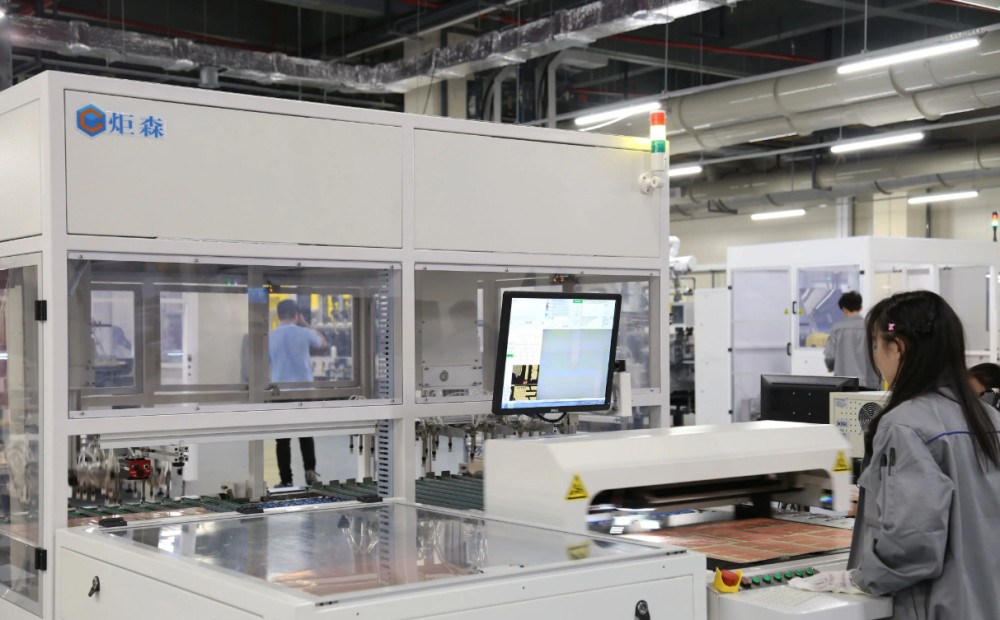
Key Step Explanations:
Circuit Fabrication: Includes Dry Film Lamination → Exposure → Development → Etching → Film Stripping
Surface Treatment: Optional processes such as Electroless Nickel Gold Plating, Tin Immersion, OSP (Organic Solderability Preservative), etc.
Coverlay Lamination: Requires hot pressing or UV curing processes
Profile Machining: Select stamping/milling/laser cutting according to requirements
Note: The actual process may add the following steps due to the complexity of the process (such as multilayer boards, rigid-flex boards):
- Lamination (for multilayer boards)
- Laser Blind Vias (for HDI boards)
- Selective Gold Plating (for key areas)
- Conformal Coating (for special protection)
Please feel free to let me know if you need a more detailed flowchart or specific process instructions for a certain step!
The materials of flexible printed circuit boards (FPCs) mainly include the following categories:
Substrate Materials
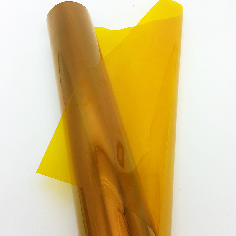
- Polyimide (PI) Film: It has excellent heat resistance, moisture resistance, electrical insulation properties, and mechanical properties. It can maintain stability in high-temperature environments and is a commonly used substrate material for flexible printed circuit boards.
- Polyester (PET) Film: It has a lower cost and has certain flexibility and electrical properties. However, its heat resistance and mechanical strength are not as good as those of polyimide film, and it is suitable for occasions with relatively low performance requirements.
Metal Materials
- Copper Foil: It is the main material for the conductive circuits in flexible printed circuit boards, with good electrical conductivity, thermal conductivity, and ductility. According to the manufacturing process, it can be divided into electrolytic copper foil and rolled copper foil. Electrolytic copper foil has a lower cost, and rolled copper foil has better performance, especially in terms of flexibility and tensile resistance.
Cover Layer Materials
- Coverlay: It is generally made of polyimide or polyester film, with an adhesive layer coated on the surface. It is used to cover and protect the circuits, enhance the insulation and moisture resistance of the printed circuit board, and also play a role in beautification.
- Solder Mask Ink: Its function is similar to that of the coverlay. It has good insulation and solder resistance properties, which can prevent the splashing of solder and short circuits during soldering, and at the same time provide certain mechanical protection.
Adhesive Materials
- Adhesives: They are used to bond different materials such as copper foil and the substrate, coverlay and the printed circuit board, etc. They are required to have good bonding strength, temperature resistance, and moisture resistance. Common adhesives include acrylate-based, epoxy resin-based adhesives, etc.
Other Materials
- Reinforcement Materials: In some specific parts of the flexible printed circuit board, such as connection points and interfaces, reinforcement materials will be used to increase strength and hardness and prevent these parts from breaking or deforming during use. Commonly used reinforcement materials include polyimide, fiberglass cloth, etc.
- Surface Treatment Materials: In order to improve the solderability, oxidation resistance, and electrical properties of the printed circuit board, its surface will be treated. For example, various chemical reagents and materials used in processes such as electroless nickel gold plating, tin immersion, and electroplating hard gold.
What should be paid attention to when selecting flexible circuit boards materials?
When selecting materials for flexible printed circuit boards (FPCs), it is necessary to comprehensively consider the application scenarios, performance requirements, and cost factors. The following are the key considerations:
1. Application Environment and Performance Requirements
- Temperature Range: Select the substrate material according to the usage scenario.
- High-temperature Environment (such as automotive electronics and industrial equipment): Give priority to polyimide (PI) film, which can withstand temperatures above 260°C.
- Low-temperature or General Environment (such as consumer electronics): Polyester (PET) film has a lower cost, but its heat resistance is poor (≤150°C).
- Mechanical Stress: For scenarios with frequent bending or folding, materials with high flexibility (such as rolled copper foil and PI substrate) should be selected.
- Chemical Resistance: In environments where contact with corrosive substances should be avoided, a surface treatment process with strong chemical resistance (such as electroless nickel gold plating) should be chosen.
2. Matching of Material Characteristics
- Substrate Materials:
- PI: It has excellent comprehensive performance but is costly.
- PET: It has a low cost and is suitable for static or low-stress scenarios.
- Types of Copper Foil:
- Electrolytic Copper Foil: It has a low cost and is suitable for ordinary circuits.
- Rolled Copper Foil: It has better flexibility and tensile resistance and is suitable for high-frequency or dynamically bending scenarios.
- Cover Layer Materials:
- Coverlay (PI/PET): It provides insulation and protection and needs to match the substrate material.
- Solder Mask Ink: It is used for local protection, and its adhesion and solder resistance need to be considered.
3. Process Compatibility
- Manufacturing Process: Ensure that the materials are compatible with the production process (such as drilling, etching, and lamination).
- For example, for multilayer boards, an adhesive with high bonding strength (such as epoxy resin-based adhesive) should be selected.
- Surface Treatment: Select the process according to the soldering requirements.
- Electroless Nickel Gold Plating (ENIG): It is suitable for complex soldering; tin immersion has a low cost but weak oxidation resistance.
4. Reliability and Service Life
- Aging Resistance: For long-term use, the anti-yellowing and anti-ultraviolet capabilities of the materials need to be considered (for example, PI is better than PET).
- Reinforcement Design: Add reinforcement materials (such as PI or fiberglass cloth) at the connection points or interfaces to enhance the mechanical strength.
5. Cost Control
- Material Cost: PI substrates and rolled copper foils are relatively expensive, and it is necessary to balance performance and budget.
- Processing Cost: Complex processes (such as laser blind vias and selective gold plating) will increase the cost, and the design needs to be simplified according to the requirements.
6. Regulatory and Environmental Requirements
- Comply with environmental protection standards such as RoHS and REACH and avoid the use of hazardous substances.
- Consider the recyclability of materials to reduce the impact on the environment.
Conclusion: The selection of materials for flexible printed circuit boards should focus on the application scenarios and balance performance, process, and cost. It is recommended to closely cooperate with material suppliers and manufacturers and verify the reliability of the selected materials through sample testing.
Advantages of Flexible Printed Circuit Boards (FPCs) Illustrated in Multiple Aspects
1. Physical Performance Advantages
- High Flexibility and Adaptability
Can be bent, folded, or even twisted, adapting to complex spaces (such as the curved surface fitting of wearable devices and the compact layout of automotive wiring harnesses).
- Ultra-thin and Lightweight
Usually only 0.05–0.3mm thick, significantly reducing the volume and weight of devices (such as mobile phone battery connections and the internal wiring of Bluetooth headphones).
- Vibration and Impact Resistance
Flexible materials buffer mechanical stress, making them suitable for vibrating environments such as sports equipment and in-vehicle electronics.
2. Electrical and Signal Performance
- High-density Interconnection
Supports multi-layer stacking (such as 3–8 layers), achieving a small pitch (minimum line width/line spacing ≤ 50μm), meeting the high-density requirements of 5G modules, camera modules, etc.
- Low Signal Loss
In high-frequency transmission (such as in the millimeter-wave band), the signal attenuation is lower than that of rigid boards, suitable for 5G antennas and high-speed data transmission.
- Optimized Electromagnetic Shielding
A shielding layer (such as a metal foil) can be integrated to reduce electromagnetic interference (EMI) and improve the signal stability of medical devices and avionics.
3. Thermal Management Capability
- Efficient Heat Dissipation
Thermally conductive PI substrates or metal-based flexible boards (such as aluminum-based FPC) can quickly conduct heat, solving the heat dissipation problems of LED displays and wireless charging modules.
- High-temperature Resistant Materials
The PI substrate can withstand soldering at 260°C, suitable for automotive engine peripheries and industrial high-temperature environments.
4. Manufacturing and Cost Advantages
- Simplified Assembly Process
The pre-shaped design reduces the number of soldering points and lowers labor costs (such as the keyboard cables of laptops).
- Modular Design
Can be customized into complex shapes (such as L-shaped, Z-shaped), directly replacing multiple wiring harnesses and saving assembly time.
- Economy of Mass Production
The roll-to-roll (R2R) production process improves efficiency and is suitable for large-scale manufacturing (such as the annual output of mobile phone FPCs exceeding 100 million pieces).
5. Reliability and Service Life
- Fatigue Resistance
The dynamic bending life can reach more than 100,000 times (such as the FPC at the hinge of a foldable mobile phone).
- Environmental Adaptability
Has a wide temperature resistance range (-55°C to +150°C), is moisture-proof and corrosion-resistant, and is suitable for outdoor devices and marine electronics.
6. Environmental Protection and Sustainability
- Recyclable Materials
Halogen-free substrates (such as PI/PET) meet the RoHS standard, and some enterprises have achieved the recycling and reuse of FPC.
- Reduced Resource Consumption
Replacing traditional wiring harnesses can save more than 30% of materials and reduce carbon emissions.
7. Innovative Application Scenarios
- Wearable Devices
Flexible sensors that fit the skin (such as heart rate monitoring in smart bracelets).
- Medical Field
Implantable devices (such as the leads of cardiac pacemakers), flexible electrode patches.
- Smart Cars
Curved dashboard screens, flexible antennas of the ADAS system.
Summary: Through physical flexibility, optimized electrical performance, manufacturing economy, and environmental protection features, flexible printed circuit boards have become one of the core technologies for the miniaturization and intelligence of modern electronic devices, and are particularly indispensable in emerging fields (such as foldable screens and metaverse hardware).
Typical Applications and Specific Cases of Flexible Printed Circuit Boards (FPCs) in Different Fields
1. Consumer Electronics Field
- Smartphones
- Application Areas: Screen cables, battery connections, camera modules, fingerprint recognition modules.
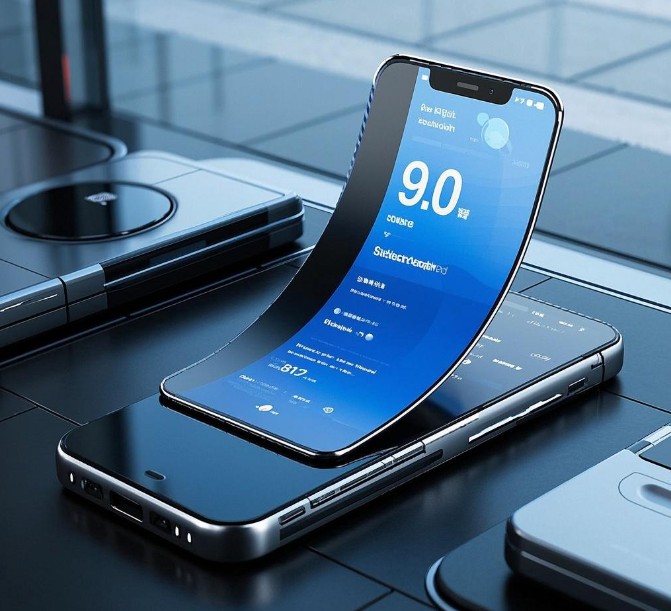
- Case: The Huawei Mate X series of foldable smartphones use multi-layer PI substrate flexible printed circuit boards, which can achieve more than 100,000 dynamic bends at the hinge, supporting the folding of the screen.
- Technical Features: Ultra-thin (0.05mm), high density (line width ≤ 50μm), and an integrated shielding layer to reduce signal interference.
- Laptops
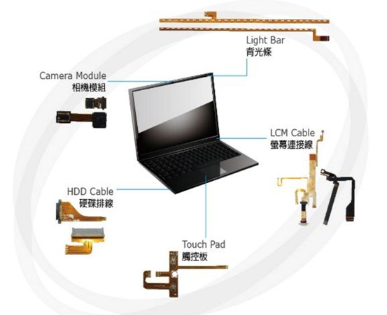
- Application Areas: Keyboard cables, touchpad connections, and screen backlight power supply.
- Case: The butterfly keyboard of the Apple MacBook Pro uses FPC instead of traditional wiring harnesses, saving space and improving reliability.
2. Automotive Electronics Field
- Battery Management System (BMS) of New Energy Vehicles
- Application Areas: Battery cell voltage collection, temperature sensor connections.
- Case: The battery pack of the Tesla Model 3 uses flexible FPC to replace the wiring harness, reducing the number of connectors by 90% and lowering the risk of failure.
- Technical Features: High-temperature resistant PI substrate (-40°C to +125°C), anti-vibration design.
- In-vehicle Displays
- Application Areas: Curved dashboards, central control screens.
- Case: The Hyperscreen super large integrated screen of the Mercedes-Benz EQS uses FPC to achieve curved surface fitting, supporting multi-zone touch control and high-resolution display.
3. Medical Equipment Field
- Implantable Medical Devices
- Application Areas: Heart pacemaker leads, nerve stimulator electrodes.
- Case: The flexible electrodes of the Medtronic heart pacemaker use ultra-thin FPC, reducing the stimulation to human tissues and supporting long-term implantation.
- Technical Features: Biocompatible materials (such as polyimide coating), resistant to body fluid corrosion.
- Medical Imaging Equipment
- Application Areas: MRI equipment coils, ultrasound probe cables.
- Case: The flexible MRI coils of General Electric (GE) use FPC, which can fit the curved surface of the human body and improve the imaging accuracy.
4. Industrial Control Field
- Robot Sensors
- Application Areas: Joint torque sensors, flexible pressure sensors.
- Case: The flexible tactile sensors of Boston Dynamics robots use FPC, which can sense the contact force in real-time and optimize the motion control.
- Technical Features: Resistant to high and low temperatures (-55°C to +150°C), resistant to industrial dust pollution.
- Industrial Automation Equipment
- Application Areas: Servo motor encoder connections, internal wiring of control cabinets.
- Case: The Siemens PLC system uses FPC to replace hard wires, reducing the weight and complexity of the wiring harness and improving the compactness of the equipment.
5. Wearable Device Field
- Smart Watches/Fitness Trackers
- Application Areas: Heart rate sensors, blood oxygen detection modules, screen drivers.
- Case: The flexible FPC of the Xiaomi Mi Band 7 fits the curved surface of the wrist, integrating photoelectric sensors and LED lights to achieve high-precision health monitoring.
- Technical Features: Waterproof design (IP68), supporting more than 100,000 bending lifetimes.
- VR/AR Devices
- Application Areas: Micro-display cables, eye tracking sensors.
- Case: The flexible FPC of the Meta Quest 3 connects the OLED screen and the processor, achieving a 2K resolution display in a narrow space.
6. Aerospace Field
- Aircraft Wiring Harnesses
- Application Areas: Wing sensor networks, cockpit instrument connections.
- Case: The Boeing 787 Dreamliner uses FPC to replace traditional wiring harnesses, reducing the weight by 30% and lowering fuel consumption.
- Technical Features: Radiation-resistant materials (such as polytetrafluoroethylene substrate), passing the aviation-grade flame-retardant certification.
- Satellite Electronic Systems
- Application Areas: Solar panel circuits, attitude control system cables.
- Case: The flexible solar arrays of SpaceX Starlink satellites use FPC, which can be folded and stored and deployed in space.
7. Environmental Technology Field
- Flexible Solar Cells
- Application Areas: Wearable power generation devices, integration with building glass.
- Case: The flexible gallium arsenide solar thin-film battery of Hanergy (Hanergy) uses an FPC substrate, which can be bent and attached to the surface of a backpack to power outdoor devices.
- Technical Features: Lightweight (≤100g/m²), with a photoelectric conversion efficiency of up to 30%.
- Smart Packaging
- Application Areas: Food freshness monitoring labels, logistics tracking sensors.
- Case: The smart packaging of Nestlé coffee uses FPC to integrate humidity sensors, and the status of the food inside the packaging can be read via mobile phone NFC.
Summary: Through characteristics such as flexibility, thinness, and high reliability, flexible printed circuit boards have achieved innovative applications that traditional rigid boards cannot replace in fields such as consumer electronics, automobiles, and medicine. They play a key role especially in cutting-edge technologies such as foldable screens, implanted medicine, and new energy.
