Description
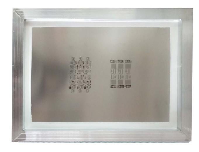
pcb Stencil
Laser-cut stainless steel+ni-polished
Framed stencil(29x29)inch/736x736mm&foil Thickness=100micron
Frame height or thickness=30-40um,Frame border width=40mm
All solder paste apertures up to 0% of its actual size
trapezdidal shaped apertures required
Laser PCB stencil is a kind of special mold used for PCB printing. The main function is to assist the deposition of solder paste and transfer the exact amount of solder paste to the exact position on the blank PCB. It has the following characteristics:
- High precision: Using laser cutting technology, the opening position has extremely high precision, and the overall error is ≤ ±4 μm.
- Good demolding property: The trapezoidal opening is beneficial for demolding and can be precisely cut.
- Smooth hole wall: After electrochemical treatment, the hole wall is smooth with a roughness of <3 μm, which is beneficial for the release of solder paste.
The production of laser PCB stencil requires the following materials:
- PCB file: Ensure the correct version, without deformation, damage, or fracture.
- Data file: Supports multiple CAD data formats such as GERBER, HPGL, *.JOB, *.PCB, *.GWK, *.CWK, *.PWK, *.DXF, *.PDF, etc.
- GERBER file: A file that converts PCB information into electronic data that can be recognized by various plotters, including X and Y coordinates and additional commands.
When using a laser PCB stencil, the following points should be noted:
- Regular cleaning: Use professional cleaning equipment such as pneumatic stencil cleaning machines or electric stencil cleaning machines to ensure the cleanliness of the stencil.
- Avoid collision: During production, transportation, and use, avoid the stencil from being collided to avoid affecting its precision and service life.
- Proper storage: The stencil should be stored in a dry and clean environment to avoid moisture and contamination.


