Description
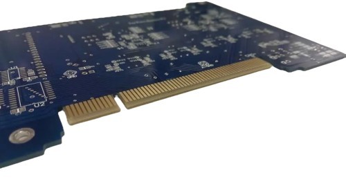
PCB gold finger connector means PCB gold finger connector, also known as edge connector. It refers to a row of golden conductive contacts on a PCB (printed circuit board) for connection.
The main function of the gold finger is to achieve conductive connections between different PCBs or between PCBs and other devices. Gold is chosen as the coating material because of its superior electrical conductivity, oxidation resistance and wear resistance.
There are usually several surface treatment methods for gold fingers as follows:
1. Electroplated nickel-gold: The thickness can reach 3-50u", with good electrical conductivity, oxidation resistance and wear resistance. It is often used in PCBs that need frequent plugging and unplugging or mechanical friction. However, due to the high cost of gold plating, it is generally only used for local gold plating treatment such as gold fingers.
2. Immersion gold: The thickness is usually 1u" and the maximum can reach 3u". It has good electrical conductivity, flatness and solderability, and is often used in high-precision PCBs with designs such as key positions, bonded ICs, BGAs, etc. For PCB with gold fingers that do not have high requirements for wear resistance, the whole board immersion gold process can also be selected. Its cost is much lower than the electroplated nickel-gold process, and the color is golden.
Common issues related to "PCB gold finger connector" include aspects such as design, production, and manufacturability testing. Here are some specific contents:
- PCB gold finger connector design aspects:
- PCB gold finger connector bevel design: Ensure there is a safe distance between the "gold finger" and the board edge. The conventional bevel angle is 45 degrees. If the "gold finger" is too close to the board edge, copper should be removed based on the finished board thickness and bevel angle to avoid copper exposure. If you don't want the "gold finger" to be shortened, a safe distance from the board edge can be designed based on specific parameters.
- PCB gold finger connector solder mask opening design: For ease of card insertion, no solder mask is applied at the "gold finger" position, and a full open window treatment is required. The window opening at the "gold finger" and tin finger area should be about 10 MIL larger than the board edge; the solder mask opening is 4 MIL larger than the circuit on one side. Also, pay attention to the distance of the window opening from the copper foil around the "gold finger" to avoid copper exposure. Otherwise, copper should be removed. Vias within 2MM of the "gold finger" are not allowed to have window openings.
- PCB gold finger connector board corner treatment design: The outline line at the "gold finger" position needs to be chamfered, either with a bevel or a fillet. If the corner of the outline board is not chamfered, the right angle may damage the card slot during insertion and removal, reducing product reliability.
- PCB gold finger connector circuit layer copper plating design: It is best not to apply copper plating in the outer surface "gold finger" area. If two or more are in the same network, copper plating will connect them together, affecting the convenience of insertion and removal.
- PCB gold finger connector long and short "gold finger" design: The main lead of the long and short "gold finger" is 40 mil, the secondary lead is 20 mil, the connection point is 6 mil, and the spacing between the "gold finger" pad and the 20 mil lead is 8 mil. After adding the leads, the main lead needs to be moved to a spacing of 8 mil from the long "gold finger". When the main lead enters the single board, if there is a large groove next to the "gold finger", the lead should be made into a fillet rather than a right angle.
- Panel design: When the single board size of the "gold finger" board is less than 40*40MM, the beveling must be done first and then the single board shape is milled. Before beveling, the board is milled into a long strip shape. CAM needs to design positioning holes on both electroplating edges for the second shape positioning during milling, and arrange the CNC process before beveling in MI. Automatic beveling must ensure that the width of the "gold finger" is more than 40MM. The "gold finger" board uses an inverted panel assembly method to expose the "gold finger" outward. When assembling PNL, the "gold finger" should be inward as much as possible to facilitate adding electroplated gold leads.

- PCB gold finger connector production aspects:
- The production process of broken "gold finger" includes steps such as material opening, inner layer imaging, inner layer etching, inner layer AOI, browning, lamination, drilling, copper deposition, panel plating, outer layer imaging, pattern plating, outer layer etching, outer layer AOI, solder mask printing, solder mask imaging, solder mask inspection, character printing, solder mask printing 2, solder mask imaging 2, immersion gold, gold finger plating, surface QC inspection, film removal 1, outer layer imaging 2, development 2, outer layer etching 2, film removal, milling, "PCB gold finger" chamfering, electrical testing, final inspection, and shipping.
- CAM compensation: When engineering technology CAM prepares the data of multilayer boards with "gold finger" (gold plug) process for ordinary products, the inner layer copper stack in the "gold finger" (gold plug) area is 80 mil, and for photoelectric products and memory sticks, it is 40 mil. For boards that do not have the "PCB gold finger" process but require beveling, the circuit copper stack also needs to be done as per the requirements of the "gold finger". The lead width of the "PCB gold finger" is 12 mil and is compensated together with the circuit. The current "PCB gold finger" width is 40 mil, and the length is the same as the lead "gold finger". For photoelectric products with the "PCB gold plating + gold finger" process, the solder pad circuit is not compensated. The distance of the "gold finger" from the board edge is ≥ 0.5MM. For board thickness tolerance of +/- 0.1MM, auxiliary copper should be added in the panel assembly gap outside the "gold finger", and 0.4MM non-metallized holes should be added at the corners of the shape of the "gold finger" area.
- The PCB gold finger connector thickness of electroplated nickel-gold can reach 3-50u", with superior electrical conductivity, oxidation resistance, and wear resistance. It is often used in "gold finger" PCBs that need frequent insertion and removal or PCBs that undergo frequent mechanical friction. However, due to the high cost of gold plating, it is only used for local gold plating treatment. The thickness of immersion nickel-gold is usually 1u", and the maximum can reach 3u". It has superior electrical conductivity, flatness, and solderability and is widely used in high-precision PCBs with designs such as key positions, bonded ICs, and BGAs. For "gold finger" PCBs with low requirements for wear resistance, the whole board immersion gold process can also be selected. The cost is much lower than the electroplated gold process, and the color is golden.
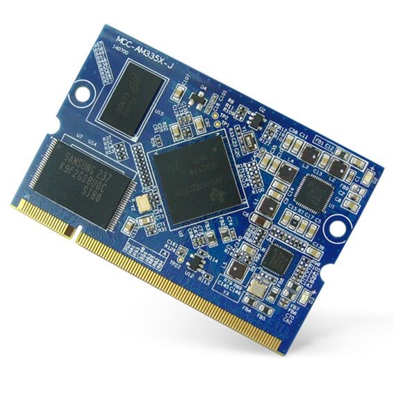
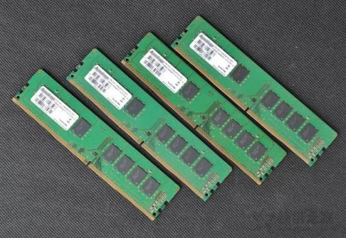
"PCB gold finger connector" can be called "PCB gold finger connector" or "PCB gold finger connection component" in Chinese. It is the connector of the PCB board as the export for external connection networks. Usually, it refers to a row of golden conductive contacts on the edge of the PCB for compressive contact and conductive interconnection with the connector spring. The gold finger has good electrical conductivity, wear resistance, oxidation resistance, and corrosion resistance. It is often used in the connection between computer memory sticks, graphics cards, sound cards, network cards, etc. and slots, or for connecting computer peripherals and the motherboard, such as speakers, subwoofers, scanners, printers, and display devices. Common types of gold fingers include regular gold fingers (flush fingers), long and short gold fingers (uneven gold fingers), and segmented gold fingers (discontinuous gold fingers), etc.

To increase the wear resistance of the gold finger, hard gold (gold compound) is usually electroplated. The "gold" of the gold finger is generally not pure gold because pure gold is relatively soft. Instead, electroplated "hard gold", an alloy of gold and other metals, is mostly used. At the same time, all layers inside the gold finger usually require copper reduction treatment. The copper reduction width is generally greater than 3mm. Half-finger copper reduction or entire finger copper reduction can be selected. In practical applications, attention should also be paid to avoiding oxidation of the gold finger, such as maintaining a good storage environment and avoiding direct contact with the gold finger by hand. Methods such as cleaning, polishing, and applying protective coatings can also be used to deal with oxidation issues.
In the production process of PCB gold fingers connector, the common problems that need attention include:
1. PCB gold fingers connector surface cleanliness: During the production process, it is necessary to avoid the surface of the gold fingers from being contaminated with oil, dust or other pollutants, which will affect its electrical conductivity and contact performance.
2. Gold plating quality: Ensure that the thickness of the gold plating layer is uniform and avoid local unevenness in thickness. Otherwise, it may lead to inconsistent wear resistance and electrical conductivity.
3. PCB gold fingers connector anti-oxidation treatment: Gold fingers are prone to oxidation during production and storage. Effective anti-oxidation measures need to be taken, such as using antioxidants or storing them in a specific environment.
4. PCB gold fingers connector line alignment: The gold fingers and the lines on the PCB must be precisely aligned; otherwise, it may cause poor contact or signal transmission problems.
5. PCB gold fingers connector bevel processing: The bevel angle and size of the gold fingers should meet the design requirements to ensure smooth insertion and removal without damaging the connector.
6. PCB gold fingers connector solder resist control: In the gold finger area, the coverage of the solder resist layer should be precisely controlled to prevent the residue of the solder resist from affecting the contact.
7. PCB gold fingers connector coating adhesion: Ensure that there is a good adhesion between the gold coating and the PCB substrate to prevent the coating from peeling off.
8. PCB gold fingers connector stress control: In the heat processing and other links during the production process, the stress should be well controlled to avoid adverse effects on the structure and performance of the gold fingers.
9. PCB gold fingers connector testing and inspection: Conduct strict electrical performance tests and appearance inspections to promptly discover and eliminate defective products.
10. Storage conditions: The PCB gold fingers after production should be stored in a dry and corrosive gas-free environment to prevent moisture or oxidation.
Gold fingers have different classifications. Common classifications are as follows:
1. Ordinary gold fingers (flat fingers): Arranged neatly on the edge of the board, and the length and width are the same as the rectangular pads.
2. Segmented gold fingers (discontinuous gold fingers): The length of the rectangular pad is different at the position on the edge of the board, and the front section is disconnected.
3. Long and short gold fingers (i.e. uneven gold fingers): Rectangular pads of different lengths located at the edge of the board.
Gold fingers are widely used in various electronic devices, such as computer memory sticks, graphics cards, smart phones, smart watches, etc., to achieve signal transmission and connection between different circuit modules inside the device. In these devices, the gold finger, as a key part of the connection, ensures the stable transmission of signals and the normal operation of the device. At the same time, because the gold finger needs to be plugged and unplugged frequently, its good wear resistance and oxidation resistance help to extend the service life of the device and ensure the reliability of the connection.


