Description
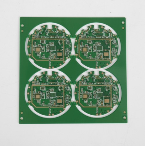
What are blind and buried vias HDI PCB?
HDI PCB (High Density Interconnect Printed Circuit Board), blind and buried vias are one of its key features.
A blind via is a via that only connects the surface layer and the inner layer of the PCB. One end of it is visible on the surface of the PCB, and the other end is in the inner layer. A buried via is completely located in the inner layer of the PCB, and neither end can be seen on the surface.
The use of blind and buried vias can greatly increase the wiring density of the PCB. They enable signals to be transmitted between different inner layers, reducing the wiring space occupation on the surface of the PCB and contributing to a more compact design.
In terms of the manufacturing process, the production of blind and buried vias requires high-precision drilling and plating technologies. This increases the production cost but also makes it possible to achieve high-performance and miniaturized electronic products.
Blind and buried vias can also improve the electrical performance of the PCB. By shortening the signal transmission path, signal delay and loss are reduced, and the integrity and reliability of the signal are improved.
In the design of multi-layer PCBs, a reasonable planning of the layout and quantity of blind and buried vias can effectively optimize the distribution of power and ground, reducing noise and electromagnetic interference.
In conclusion, the application of blind and buried vias enables HDI PCB to play an important role in modern electronic devices, meeting the requirements for smaller size, higher performance and more complex functions.
What are the classifications of blind and buried via PCB?
Blind and buried via PCBs can usually be classified in the following ways:
1. According to the number of blind and buried vias: They can be classified as PCB with a small number of blind and buried vias and PCB with a large number of blind and buried vias. The former has a relatively small number of blind and buried vias, while the latter has a larger number.
2. According to the size of blind and buried vias: They can be classified as PCB with small-aperture blind and buried vias and PCB with large-aperture blind and buried vias. The small-aperture ones usually have higher requirements for the manufacturing process.
3. According to the number of layers: There are multi-layer blind and buried via PCBs and blind and buried via PCBs with fewer layers. The multi-layer structure is more complex, and the design and manufacturing difficulty is also relatively larger.
4. According to the application field: For example, blind and buried via PCBs used in the communication field, the computer field, the consumer electronics field, etc. Different fields have different requirements for their performance and specifications.
These classification methods are helpful for selecting and designing the appropriate blind and buried via PCBs according to specific needs and application scenarios.
What are the differences between HDI blind and buried vias and ordinary electroplated through holes?
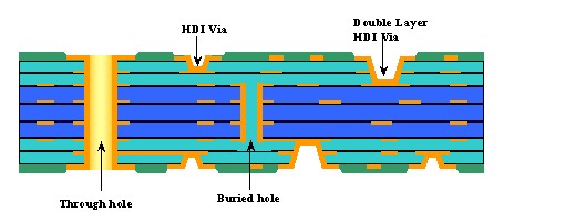
The main differences between HDI blind and buried vias PCB and ordinary electroplated through holes PCB are as follows:
1. Connection structure: Ordinary electroplated through holes penetrate the entire PCB board, connecting from the top layer to the bottom layer; while HDI blind vias only connect the surface layer and inner layers of the PCB, and buried vias connect between the inner layers.
2. Wiring density: HDI blind and buried vias help increase the wiring density of the PCB because they do not occupy the space on the PCB surface like ordinary through holes, allowing the PCB to be designed more compactly.
3. HDI blind and buried vias PCB Signal transmission performance difference: Since blind and buried vias shorten the signal transmission path, they can reduce signal delay and loss, and improve signal integrity and transmission speed. In contrast, the signal transmission path of ordinary through holes is longer, which may lead to more signal problems.
4. HDI blind and buried vias PCB manufacturing process difference: The manufacturing process of HDI blind and buried vias is more complex and precise, requiring a higher technical level and more advanced equipment. The manufacturing of ordinary electroplated through holes is relatively simple.
5. Cost difference of HDI blind and buried vias PCB: The manufacturing cost of HDI blind and buried via PCBs is usually higher than that of PCBs with ordinary electroplated through holes due to their complex process and high precision requirements.
In conclusion, HDI blind and buried vias have advantages in terms of wiring density and signal performance, but they also have higher costs and manufacturing difficulties. They are suitable for high-end electronic products with high requirements for performance and space; ordinary electroplated through holes have lower costs and relatively simple manufacturing, and are suitable for some products with less demanding performance requirements.
Why are PCB boards designed with blind and buried vias?
The PCB boards are designed with blind and buried vias mainly for the following reasons:
1. Improving wiring density: Blind and buried vias can achieve connections between different layers without occupying the surface space of the PCB, thus making more space available for surface wiring and facilitating a more complex circuit layout within a limited area.
2. Improving signal transmission performance of HDI blind and buried vias PCB: They shorten the signal transmission path, reduce signal delay, loss and reflection, and improve the integrity and transmission speed of the signal, especially suitable for high-frequency and high-speed circuits.
3. Achieving thinner PCB designs: They can reduce the number of layers of the PCB and make the PCB board thinner, meeting the trend of thinner and lighter electronic products.
4. Reducing electromagnetic interference HDI blind and buried vias PCB : They help optimize the circuit layout and reduce the interference between different lines, thereby reducing electromagnetic interference and improving the stability and reliability of the circuit.
5. Enhancing the confidentiality of the circuit: Since blind and buried vias are located inside the PCB and are not easily directly observed and analyzed, they have certain advantages for some applications that have confidentiality requirements for the circuit design.
In conclusion, the design of blind and buried vias can enhance the performance of the PCB, reduce its size and meet specific circuit design requirements.
How to reduce the production cost of blind and buried via HDI PCB?
Here are some possible ways to reduce the production cost of blind and buried via HDI PCB:
1. Optimize the design of HDI blind and buried vias PCB: At the design stage, by rationally planning the circuit layout, reducing the number of unnecessary blind and buried vias, and optimizing the via hole size, etc., the manufacturing difficulty and material cost can be reduced.
2. Improve HDI blind and buried vias PCB production efficiency: Adopt advanced production equipment and processes, increase the degree of automation in production, reduce the production cycle and manual intervention, thereby reducing the production cost per unit product.
3. Raw material procurement of HDI blind and buried vias PCB: Establish long-term cooperative relationships with reliable suppliers and obtain more favorable raw material prices through bulk purchasing.
4. Improve the yield rate: Strengthen quality control during the production process, reduce the generation of waste and defective products, and increase the qualification rate of products.
5. Process improvement: Continuously research and improve the production process to reduce process costs, such as optimizing process parameters such as drilling and electroplating.
6. Employee training: Improve the skill level and operational proficiency of employees to reduce the increase in costs caused by operational errors.
7. Supply chain management: Optimize the HDI blind and buried vias PCB's supply chain to reduce logistics and inventory costs.
It should be noted that while reducing costs, it is necessary to ensure that the quality and performance of the PCB are not affected to meet the usage requirements of the product.
