Description
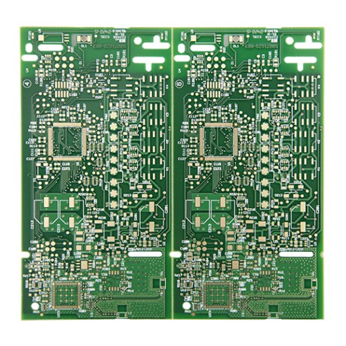
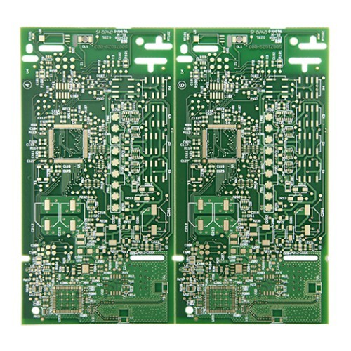
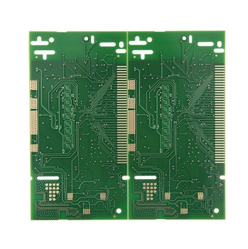
HDI PCB (High Density Interconnect Printed Circuit Board) is a kind of printed circuit board that uses micro-blind and buried hole technology and can integrate more circuits and components in a smaller space.
The following is the manufacturing process of HDI PCB:
1. HDI PCB layout : The first step in PCB manufacturing is to organize and inspect the PCB layout. The PCB manufacturing factory will convert the CAD file into Extended Gerber RS-274X or Gerber X2 format, and then the factory's engineers will check whether the PCB layout conforms to the manufacturing process and whether there are any defects.
2. HDI PCB Core plate manufacturing: Clean the copper clad laminate to remove dust to avoid short circuits or open circuits in the circuit. Then cover the copper clad laminate with a photosensitive film. The photosensitive film will solidify when exposed to light, forming a protective film on the copper foil of the copper clad laminate. Next, stack the two layers of PCB layout films and the double-layer copper clad laminate together, and insert the upper PCB layout film to ensure that the positions of the two layers of PCB layout films are precisely stacked. The photosensitive machine irradiates the photosensitive film on the copper foil with a UV lamp. Under the transparent film, the photosensitive film is solidified, and under the non-transparent film, the photosensitive film is still not solidified. The copper foil covered under the solidified photosensitive film is the required PCB layout circuit, which is equivalent to the role of the laser printer ink of the manual PCB. Then use an alkaline solution to wash away the non-solidified photosensitive film, and the required copper foil circuit will be covered by the solidified photosensitive film. Then use a strong alkali, such as NaOH, to etch away the unnecessary copper foil. Tear off the solidified photosensitive film to expose the required PCB layout circuit copper foil.
3. Inner layer HDI PCB layout transfer manufacturing: Firstly, make the two-layer circuits of the innermost core plate (Core). After cleaning the copper clad laminate, a layer of photosensitive film will be covered on the surface. Stack the two layers of PCB layout films and the double-layer copper clad laminate together, and insert the upper PCB layout film to ensure that the positions of the two layers of PCB layout films are precisely stacked. The photosensitive machine irradiates the photosensitive film on the copper foil with a UV lamp. Under the transparent film, the photosensitive film is solidified, and under the non-transparent film, the photosensitive film is still not solidified. The copper foil covered under the solidified photosensitive film is the required PCB layout circuit, which is equivalent to the role of the laser printer ink of the manual PCB. Then use an alkaline solution to wash away the non-solidified photosensitive film, and the required copper foil circuit will be covered by the solidified photosensitive film. Then use a strong alkali, such as NaOH, to etch away the unnecessary copper foil. Tear off the solidified photosensitive film to expose the required PCB layout circuit copper foil.
4. HDI PCB Core plate drilling and inspection manufacturing: The core plate has been successfully fabricated, and then alignment holes are drilled in the core plate for convenient alignment with other materials in the future. It should be noted that once the core plate is laminated with other layers of PCB, it cannot be modified, so the inspection is very important. The machine will automatically compare with the PCB layout drawing to check for errors.
5.HDI PCB Lamination: A new raw material called prepreg is needed. It is the adhesive between the core plate and the core plate (PCB layers greater than 4), as well as between the core plate and the outer copper foil, and also serves as insulation. The lower copper foil and two layers of prepreg have been fixed in position in advance through the alignment holes and the lower iron plate. Then place the fabricated core plate into the alignment holes. Finally, stack two layers of prepreg, one layer of copper foil, and one layer of pressure-bearing aluminum plate onto the core plate in sequence. Place the PCB plates clamped by the iron plates on the support and then send them into a vacuum hot press for lamination. The high temperature in the vacuum hot press can melt the epoxy resin in the prepreg and fix the core plates and copper foils together under pressure. After lamination is completed, remove the upper iron plate that suppresses the PCB. Then remove the pressure-bearing aluminum plate. The aluminum plate also serves to isolate different PCBs and ensure the smoothness of the outer copper foil of the PCB. At this time, the PCB taken out will be covered with a smooth layer of copper foil on both sides.
6. Drilling of HDI PCB manufacturing: To connect the four layers of non-contact copper foils in the PCB, perforations that run through the top and bottom need to be drilled first to open up the PCB, and then the hole walls need to be metallized for conductivity. Use an X-ray drilling machine to position the inner core plate. The machine will automatically find and position the hole positions on the core plate, and then drill positioning holes on the PCB to ensure that the drill passes through the exact center of the hole position when drilling in and out. Place a layer of aluminum plate on the drilling machine bed, and then place the PCB on it. To improve efficiency, 1-3 identical PCB boards will be stacked together for perforation according to the number of PCB layers. Finally, cover the top PCB with a layer of aluminum plate. The upper and lower aluminum plates are used to prevent the copper foil on the PCB from being torn when the drill bit drills in and out. In the previous lamination process, the melted epoxy resin was extruded to the outside of the PCB, so it needs to be cut off. A profile milling machine cuts the periphery of the PCB based on the correct XY coordinates of the PCB.
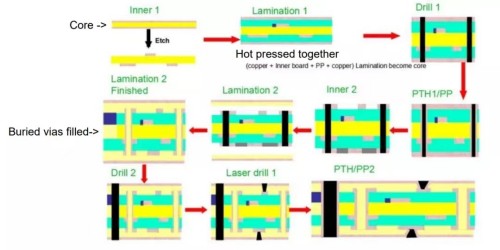
The blind and buried via structure in HDI PCB (High Density Interconnect Printed Circuit Board) is an important technology for improving the wiring density and performance of the circuit board.
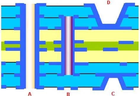
A blind via refers to a hole that is connected to the PCB surface layer at one end and the inner layer at the other end but does not penetrate the entire circuit board. For example, a blind via may connect from the outer layer to the third layer of the inner layer.
A buried via is a hole that is completely located between the inner layers of the PCB and is not connected to the outer layers at both ends. For instance, a buried via can connect the second and fourth layers of the inner layer.
The structural diagram of blind and buried vias usually shows the layer stack structure of the multilayer PCB, as well as the connection positions and methods of blind and buried vias between different layers. In the structural diagram, different colors or marks may be used to distinguish different types of holes (such as blind vias, buried vias, and through vias), and key parameters such as the diameter, depth, and plating thickness of the holes are marked.
The main advantages of the blind and buried via structure include:
- - Increasing wiring density: Allowing more circuits to be laid out in a limited space.
- - Improving signal integrity: Reducing the path length of signal transmission and lowering signal loss and delay.
- - Enhancing the performance and reliability of the circuit board.
However, the manufacturing process of blind and buried vias is relatively complex, and the cost is also high. It requires high-precision equipment and strict process control.
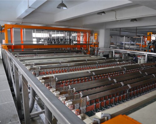
7. HDI PCB Chemical copper deposition on the hole walls manufacturing: Since almost all PCB designs use perforations to connect circuits of different layers, a good connection requires a 25-micron copper film on the hole walls. Therefore, chemical copper deposition on the hole walls is required to ensure connection quality.
Firstly, remove the resin smear to remove the epoxy resin drill dirt generated during drilling. Then, perform chemical copper deposition to deposit a thin layer of copper on the hole walls. Next, perform copper plating to thicken the copper layer on the hole walls to reach the required thickness.
8. Outer layer circuit manufacturing of HDI PCB: Cover the outer copper foil with a photosensitive film. Through processes such as exposure and development, transfer the outer layer circuit pattern to the copper foil, and then etch away the unnecessary copper foil to leave the outer layer circuit.
9. HDI PCB solder mask layer manufacturing: Apply solder mask ink on the surface of the PCB. Through processes such as exposure and development, expose the pads and holes that need to be soldered and protect other areas from oxidation and short circuits.
10. Surface treatment of HDI PCB manufacturing: Common surface treatment methods include hot air solder leveling, immersion gold, OSP, etc., to improve the solderability and corrosion resistance of the PCB.
11.HDI PCB manufacturing electrical testing: Perform electrical performance testing on the PCB to check for defects such as open circuits and short circuits.
12.HDI PCB manufacturing shape processing: According to the design requirements of the PCB, process the PCB into the required shape and size through equipment such as milling machines or punching machines.
13. HDI PCB manufacturing final inspection: Conduct a comprehensive appearance inspection and performance test on the PCB to ensure it meets quality standards.
It should be noted that the manufacturing process of HDI PCB is complex, requires high equipment and technology, and there may be some minor differences among different manufacturers.
In addition to the micro-blind and buried via technology, what other technologies can be applied to HDI PCB?
Apart from the micro-blind and buried via technology, the following technologies may also be adopted in HDI PCB:
- Laser micro-via technology: Smaller holes can be generated through laser drilling, thereby achieving a high-density circuit distribution.
- Continuous lamination technology: Used for manufacturing multi-layer PCBs to increase the number of layers and density of the circuit board.
- Via-in-pad technology: Can achieve higher density wiring and connections on the PCB.
- Electroplating via filling technology: Used to fill micro-vias and improve the reliability of electrical connections.
The application of these technologies can further enhance the performance and density of HDI PCB, meeting the requirements of modern electronic devices for smaller size and higher performance. Meanwhile, with the continuous development of technology, there may be new technologies applied in the manufacturing of HDI PCB.
Here are some methods to improve the heat dissipation performance of HDI PCB:
1. Choose high thermal conductivity materials: HDI PCB use substrate materials with good thermal conductivity, such as ceramic substrates, metal core substrates, or resin materials with high thermal conductivity coefficients.
2. HDI PCB add heat dissipation layers: Add dedicated heat dissipation layers in the PCB, such as copper foil layers or metal plates, to help heat spread quickly.
3. Optimize the wiring layout of HDI PCB : Arrange the component layout reasonably to avoid heat concentration. Distribute components with high heat generation at the edge of the PCB or in well-ventilated positions.
4. Increase the thickness of the copper foil of HDI PCB : Thicker copper foil can provide a better heat conduction path and help dissipate heat.
5. Design heat dissipation holes of HDI PCB : Drill holes on the PCB to form air convection channels and promote heat exhaust.
6. HDI PCB adopt thermal vias: Set thermal vias between different layers to conduct heat from heat-generating components to the heat dissipation layer or the outside.
7. Surface treatment of HDI PCB : Select surface treatment methods that are conducive to heat dissipation, such as silver plating or nickel plating.
8. HDI PCB install heat sinks: Install dedicated heat sinks on the PCB, such as aluminum or copper heat sinks, to enhance the heat dissipation effect.
9. Optimize the power and ground layers of HDI PCB : Design the layout of the power and ground layers reasonably to reduce local heat generation caused by uneven current density.
10. HDI PCB Software simulation analysis: Use thermal simulation software in the design stage to predict and optimize the heat dissipation performance of the PCB.
How to reduce the production cost of HDI PCB without affecting its quality?
To reduce the production cost of HDI PCB without affecting its quality, the following aspects can be considered:
1. HDI PCB optimize the design: Through careful planning of the circuit layout, reduce the number of layers, holes, and the length of lines to lower the material and processing costs.
2. Improve material utilization of HDI PCB : Select the appropriate size of the board to reduce waste generation; during the manufacturing process, precisely calculate the material usage to avoid waste.
3. Improve HDI PCB the production process: Adopt more efficient manufacturing processes and equipment to increase production efficiency and reduce the production cost per unit.
4. HDI PCB Batch production: Increase the production batch to obtain economies of scale and reduce the fixed cost per unit product.
5. Supply chain management of HDI PCB : Establish long-term cooperative relationships with reliable suppliers to strive for more favorable material prices and better services.
6. HDI PCB Quality control: Strengthen quality control during the production process, reduce the occurrence of defective and rejected products, and lower the cost increase caused by quality problems.
7. Employee training of HDI PCB : Improve the skill level and work efficiency of employees to reduce cost losses caused by operational errors.
8. HDI PCB technological innovation: Pay attention to new technologies in the industry and introduce innovative solutions that can reduce costs without affecting quality in a timely manner.
The comprehensive application of these methods can effectively reduce the production cost while maintaining the quality of HDI PCB.
What are the practical application scenarios of modern HDI PCBs (High Density Interconnect Printed Circuit Boards)?
Modern HDI PCBs have a wide range of practical application scenarios, including but not limited to the following aspects:
1. HDI PCBs apply in Smartphones and mobile devices: These devices pursue thinness, high performance and multi-functionality. HDI PCBs can meet their requirements for high-density wiring and miniaturization to support complex components such as processors, memory chips, camera modules and communication modules.
2. HDI PCBs in Tablets and laptops: To achieve thinner designs, higher processing capabilities and better graphics performance, HDI PCBs are needed to optimize the circuit board layout and signal transmission.
3. Wearable devices: Such as smart watches, fitness trackers, etc., due to limited space, HDI PCBs help integrate various sensors, microprocessors and communication modules.
4. HDI PCBs in Automotive electronics: Including automotive autopilot systems, infotainment systems, airbag control units, etc., HDI PCBs can withstand the harsh requirements of the automotive environment and provide reliable high-performance connections.

5. Medical devices in HDI PCBs: Such as portable diagnostic instruments, pacemakers, insulin pumps, etc., require high-precision and high-reliability circuit boards to ensure accurate measurement and treatment.
6. Communication equipment: Such as 5G base stations, routers, switches, etc., HDI PCBs help achieve high-speed data transmission and processing.
7. Aerospace and defense: In fields such as satellites, missile systems, aircraft avionics, etc., HDI PCBs can meet the requirements of light weight, high performance and high reliability.
8. Industrial control and automation: In factory automation equipment, robot control systems, etc., HDI PCBs help improve the integration and performance of the system.
In conclusion, as electronic devices continue to develop towards miniaturization, high performance and multi-functionality, the application of HDI PCBs is becoming more and more extensive in various fields.
