SMT Process Flow Introduction
I,surface assembly technology SMT status
SMT is currently the most popular technology and process in the electronic assembly industry. Since its introduction to the market in the early 70s, SMT has gradually replaced the traditional 'manual plug-in' wave soldering assembly method and has become the mainstream of the modern electronic assembly industry, which is known as the second revolution in electronic assembly technology. In the international arena, this assembly technology has formed a world trend, which has led to changes in the entire electronics industry.SMT also promotes and facilitates the development of electronic components to chip, miniaturization, thin, lightweight, high reliability, multi-functional direction, has become a symbol of the degree of scientific and technological progress of a country.
II, the surface assembly technology SMT process and characteristics
SMT (Surface Mount Technology) is the abbreviation or abbreviation of surface mount technology, which refers to the surface mount device (SMD) mounted on the surface of PCB (or other substrates) through certain process, equipment and materials, and welding, cleaning, testing and finally finished assembly.1,SMT process
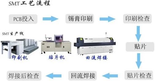
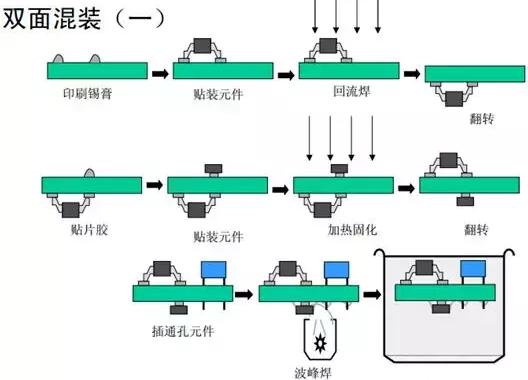
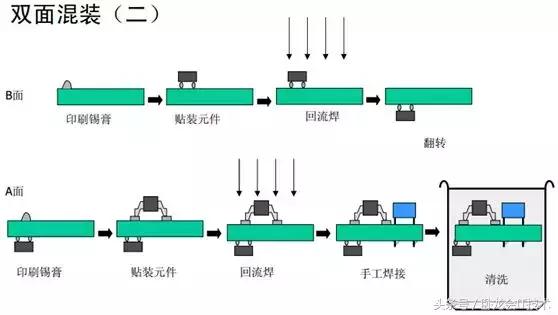
According to the assembly method can be divided into full surface assembly, single-sided mixed assembly, double-sided mixed three ways.
The main factors affecting the quality of welding: PCB design, the quality of solder (Sn63/Pb37), flux quality, the degree of oxidation of the metal surface to be soldered (component solder end, PCB solder end), process: printing, paste, welding (the correct temperature profile), equipment, management.
2, the following discussion of several factors that have a greater impact on the quality of reflow soldering.
(1) the impact of the quality of solder paste printing on the reflow soldering process.According to statistics, in the PCB design is correct, components and printed board quality is guaranteed under the premise that the quality of surface assembly problems in 70% of the quality problems out of the printing process. In the printing of misalignment, collapse, adhesion, less printing are substandard, should be reworked. Specific inspection standard should conform to the standard of IPC-A-610C.
(2) the process requirement of mounting components.
To obtain the ideal mount quality, the process should satisfy the following three elements: ① The component is correct; ② The position is accurate; ③ The pressure is suitable. The specific inspection standard shall conform to the standard of IPC-A-610C.
(3) set up the reflow soldering temperature curve of the process requirements temperature curve is the key to ensure the quality of welding.
160 ℃ before the temperature rise rate control at 1-2 ℃ / s. If the temperature rise slope speed is too fast, on the one hand, so that components and PCBs are heated too quickly, easy to damage components, easy to cause PCB deformation. On the other hand, the molten flux in the solder paste evaporates too fast, easy to spill metal components, resulting in solder balls; peak temperature is generally set at about 30-40°C higher than the melting point of the alloy (for example, the melting point of 63Sn/37Pb solder paste is 183°C, the peak temperature low should be set at about 215°C), and the reflow time is 60-90s.
Low peak temperature or short reflow time will make the welding is not sufficient to generate a certain thickness of intermetallic alloy layer. In severe cases, it will cause the solder paste not to melt. The peak temperature is too high or re-flow time is too long, so that the intermetallic alloy layer is too thick, will also affect the strength of the solder joint, and even damage components and printed boards.
3, the characteristics of SMT.
(1) high assembly density, small size of electronic products, light weight, SMD components, the volume and weight of only about 1/10 of the traditional cartridge components, generally after the use of SMT, electronic products to reduce the volume of 40% to 60%, weight reduction of 60% to 80%.(2) high reliability, strong resistance to vibration. Low defect rate of solder joints.
(3) Good high frequency characteristics. Reduced electromagnetic and radio frequency interference.
(4) Easy to realize automation and improve production efficiency.
(5) Reduce cost up to 30%~50%. Save materials, energy, equipment, manpower, time, etc.
III, the development trend of SMT surface assembly technology
1, narrow pitch technology (FPT) is the inevitable trend of SMT development
FPT refers to the pin pitch between 0.635-0.3mm SMD and length * width less than or equal to 1.6mm * 0.8mm SMC assembled on the PCB technology. Due to the rapid development of computer, communication, aerospace and other electronic technologies on the, prompting the integration of semiconductor integrated circuits is getting higher and higher, SMC is getting smaller and smaller, SMD pin pitch is also getting narrower and narrower. At present, 0.635mm and 0.5mm pin pitch QFP has become the communication devices in industrial and military electronic equipment.2, miniaturization, multi-pin, high integration is the inevitable trend of SMT package components development
Surface mount components (SMC) towards the miniaturization of large capacity direction development. At present has developed to the specification of 01005; surface mount device (SMD) towards small volume, multi-pin, high integration direction. For example, the current more widely used BGA will develop in the direction of CSP. FC (flip chip) application will be more and more.3, green lead-free soldering process is the new trend of SMT process development
Lead (Pb), is a toxic metal, harmful to the human body. And the natural environment is very destructive, for the requirements of environmental protection, especially the import of ISO14000, most countries in the world began to prohibit the use of lead in soldering materials become, that is, lead-free soldering (Lead free). Japan banned the production or sale of electronic production equipment using leaded materials for soldering in 2004. Europe and the United States in 2006 banned the production or sale of electronic production equipment using leaded materials for soldering. The use of lead-free soldering has been the trend, some large domestic electronic processing enterprises, and will accelerate the development of China's lead-free soldering.IV, SMT detailed production process
1.1 Reflow soldering process
Reflow soldering is a soft brazing process by melting the pre-printed solder paste on the PCB pads to achieve the mechanical and electrical connection between the solder end of the surface assembly components or pins and PCB pads. Its process flow is: printed solder paste - SMD - reflow soldering, as shown in the figure below.1.1.1 Solder paste printing
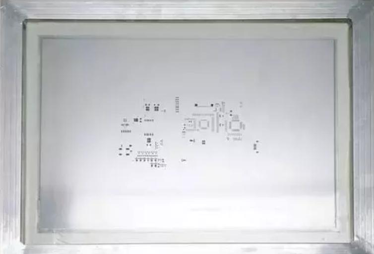
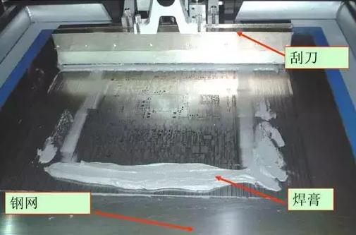
The purpose is to apply the right amount of solder paste evenly on the pads of the PCB to ensure that the SMD components and the corresponding pads of the PCB and then reflow soldering, to achieve a good electrical connection, and has sufficient mechanical strength.How to ensure the uniform application of solder paste on each pad? We need to make stencil. Solder paste is applied to each pad through the corresponding openings in the stencil, and the tin is evenly applied to each pad under the action of the squeegee. An example of the stencil diagram is shown below.
Solder paste printing diagram is shown below
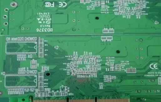
The PCB with printed solder paste is shown below
1.1.2 Placement
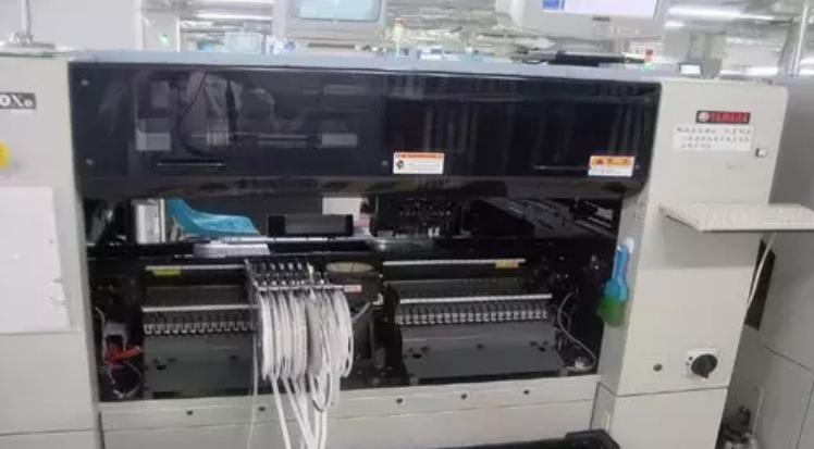
This process is to use the mounting machine to accurately mount the chip components to the corresponding position on the surface of the PCB with printed solder paste or mounting adhesive.SMD machine according to the function can be divided into two types.
A high-speed machine: applicable to mount small and large number of components: such as capacitors, resistors, etc., can also mount some IC components, but the accuracy received restrictions.
B general-purpose machine: applicable to mount heterosexual or high precision components: such as QFP, BGA, SOT, SOP, PLCC, etc.
The diagram of mounting machine equipment is shown below
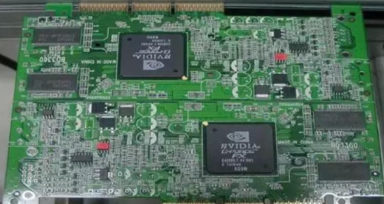
The PCB after mounting is shown as follows
1.1.3 Reflow Soldering
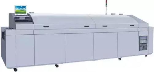
Reflow soldering is the direct translation of the English Reflow Soldring, is by melting the solder paste on the circuit board pads, to achieve the mechanical and electrical connection between the solder end of the surface assembly components and PCB pads, forming an electrical circuit.Reflow soldering as a key process in SMT production, a reasonable temperature profile setting is the key to ensure the quality of reflow soldering. Improper temperature profile will make the PCB board welding incomplete, false welding, component warping, too many solder balls and other welding defects, affecting product quality.
Reflow soldering furnace equipment diagram is shown below
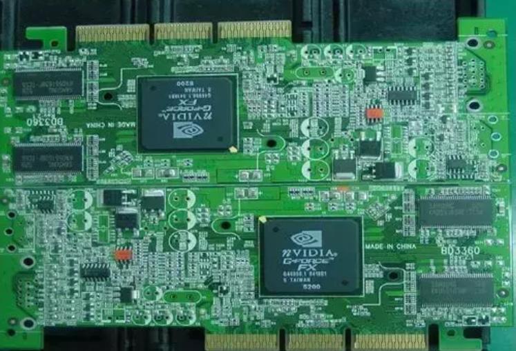
After reflow furnace, reflow soldering completed PCB as shown below
1.2 Wave soldering process
Wave soldering is generally a soldering process for plug-in devices. Is the molten liquid solder, with the help of the pump, in the solder tank liquid surface to form a specific shape of the solder wave, inserted components of the PCB in the transfer chain after a specific angle and a certain immersion depth through the solder wave peak and achieve the solder joint welding process, as shown in the figure below.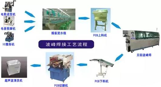
1.2.1 THC insertion and assembly technology
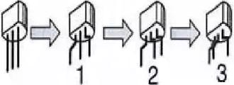
1. Component pin formingDIP devices need to be shaped for pins before insertion
(1) Manual processing of components shaping.
Bent pins can be shaped with the help of tweezers or small screwdrivers on the pins, as shown in the figure below.

Through-hole insertion technology is divided into manual insertion and automatic mechanical equipment insertion
(1) manual insertion, welding, should first insert those components that require mechanical fixing, such as power devices, heat sinks, brackets, clips, etc., and then insert the components to be fixed by welding. Do not directly touch the pins of the components and the copper foil on the printed board with your hands when inserting.
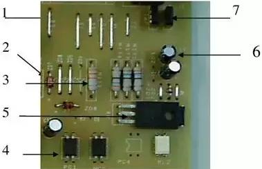
(2) mechanical automatic plug-in (referred to as AI) is a contemporary electronic product assembly in the more advanced automated production technology. Automatic mechanical equipment insertion should be inserted first those components of lower height, after installing those components of higher height, valuable key components should be put into the last insertion, heat sink, bracket, card, etc. insertion, to be close to the welding process. PCB components assembly order is shown in the figure below.
1.2.2 Wave soldering
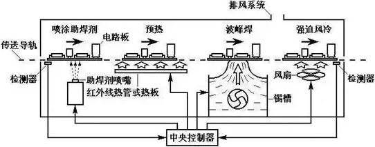
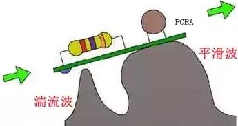
(1) Wave soldering principle of operationWave soldering is a kind of pump pressure action, so that the molten liquid solder surface to form a specific shape of the solder wave, when the assembly of the inserted components at a fixed angle through the solder wave, in the pin soldering area to form a solder joint process technology. The component is first preheated in the preheat zone of the welder during its transfer by the chain conveyor (the component preheat and the temperature it has to reach is still controlled by a predefined temperature profile). In actual welding, the preheating temperature of the component face is usually also controlled, so many devices have added corresponding temperature detection devices (e.g. infrared detectors). After preheating, the component enters the lead bath for soldering. The solder bath contains molten liquid solder, and the nozzle at the bottom of the steel bath sprays a wave of molten touching solder in a definite shape, so that the component soldering surface is heated by the solder wave as it passes through the wave, and at the same time the solder wave wets the soldering area and expands to fill it, finally realizing the soldering process. The working principle is shown in the figure below.
(2) The main components of the wave soldering machine
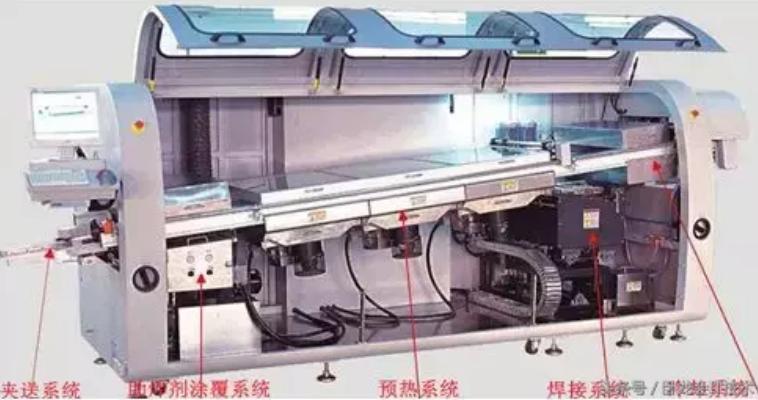
A wave soldering machine, mainly by the conveyor belt, heater, tin bath, pump, flux foaming (or spray) device and other components. It is mainly divided into flux adding area, preheating area, soldering area, and cooling area, as shown in the figure below.
1.2.3 The main difference between wave soldering and reflow soldering
The main difference between wave soldering and reflow soldering is that the heating source and the supply of solder in the solder is different. In wave soldering, the solder is preheated in the tank in a molten state, and the pumped up solder wave plays the dual role of heat source and supply of solder. The molten wave of solder makes the PCB through holes, pads and component pins heated, and also provides the solder needed to form the solder joint. In reflow soldering, the solder (solder paste) is pre-distributed quantitatively to the solder area of the PCB, and the role of the heat source during reflow is to make the solder re-melted.1.3 Selective wave soldering process introduction
Wave soldering equipment has been invented for more than 50 years, in the manufacturing of through-hole components circuit boards with high production efficiency and high yield, and other advantages, so it was once the most important welding equipment in the automated mass production of electronic products. However, there are certain limitations in its application.(1) different welding parameters.
Different solder joints on the same board due to their different characteristics (such as heat capacity, pin spacing, tin penetration requirements, etc.), the required welding parameters may be very different. However, the characteristics of wave soldering is to make all the solder joints on the whole board under the same set parameters to complete the welding, so different solder joints need to "settle" with each other, which makes wave soldering is more difficult to fully meet the welding requirements of high-quality circuit boards;.
(2) higher operating costs.
In the actual application of traditional wave soldering, flux spraying and dross generation have brought about higher operating costs; especially when lead-free soldering, because the price of lead-free solder is more than three times the price of leaded solder, dross generated by the increase in operating costs is very alarming. In addition, lead-free solder constantly melting pads on the copper, over time will make the solder composition of the tin cylinder changes, which requires regular addition of pure tin and expensive silver to solve;.
(3) maintenance and maintenance trouble.
Production of residual flux will remain in the wave soldering conveyor system, and the production of dross needs to be removed regularly, these are more complicated to the user of equipment maintenance and maintenance work.
For reasons such as these, selective wave soldering came into being.
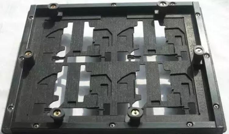
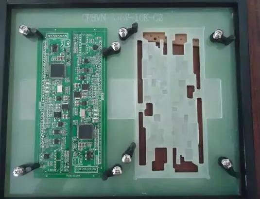
The so-called PCBA selective wave soldering or using the original tin furnace, the difference is that the board needs to be put into the over-tin furnace carrier / tray (carrier), which we often say over the furnace jig, as shown in the figure below.
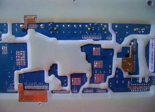
1.4 Through-hole reflow soldering process introduction
Through-hole reflow soldering is a reflow soldering process method for inserted components, mainly used in the manufacture of surface assembly boards containing a few inserts, and the core of the technology is the method of applying solder paste.1.4.1 Introduction to the process flow
According to the application method of solder paste, through-hole reflow soldering can be divided into three types: tubular printing through-hole reflow soldering process, solder paste printing through-hole reflow soldering process and molding tin sheet through-hole reflow soldering process.
1. Tubular printing through-hole reflow soldering process
Tubular printing through-hole reflow soldering process is the earliest application of through-hole components reflow soldering process, mainly used in the manufacture of color TV tuner. The core of the process is a tubular printing machine for solder paste, and the process is shown in the figure below.
2. Solder paste printing through-hole reflow soldering process
Solder paste printing through-hole reflow soldering process is currently the most applied through-hole reflow soldering process, mainly for mixed PCBA containing a small number of inserts, the process is fully compatible with the conventional reflow soldering process, no special process equipment is required, the only requirement is that the inserted components to be soldered must be suitable for through-hole reflow soldering, the process is shown in the figure below.
Formed tin through-hole reflow soldering process is mainly used for multi-pin connectors, the solder is not solder paste but formed tin, generally added directly by the connector manufacturer, the assembly can only be heated.
1.4.2 Through-hole reflow soldering design requirements
1. PCB design requirements(1) suitable for PCB thickness less than or equal to 1.6mm board.
(2) The minimum pad also 0.25mm, once again "pull" the molten solder paste, do not form tin beads.
(3) components from the board gap (Stand-off) should be greater than 0.3mm
(4) The appropriate length of the lead sticking out of the pad is 0.25~0.75mm.
(5) 0603 and other fine pitch components from the pad minimum distance of 2mm.
(6) Stencil openings can be expanded by up to 1.5mm.
(7) The diameter of the hole is the lead diameter plus 0.1~0.2mm. as shown in the figure below.
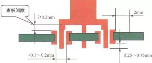
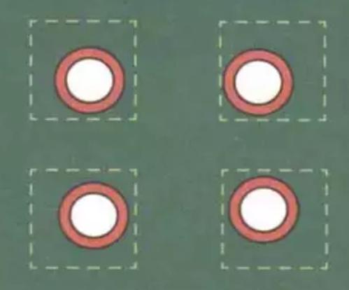
Generally speaking, in order to achieve 50% hole filling, the stencil opening must be flared out. The specific amount of flare should be decided according to the thickness of the PCB, the thickness of the stencil, the gap between the hole and the lead, and other factors.
Generally speaking, as long as the flare does not exceed 2mm, the solder paste will be pulled back and filled into the hole. It is important to note that the outward expansion cannot be pressed by the component package, or must avoid the component package body, one side of the formation of tin beads, as shown in the figure below.
1.5 PCBA conventional assembly types and process flow introduction
1.5.1 Single-sided mount
The process flow is shown in the figure below
1.5.2 Single-sided insertion
The process flow is shown in Figure 5 below
1.5.3 Double-sided placement
The process flow is shown in the figure below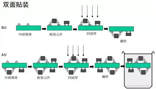
The process flow is shown in the figure below
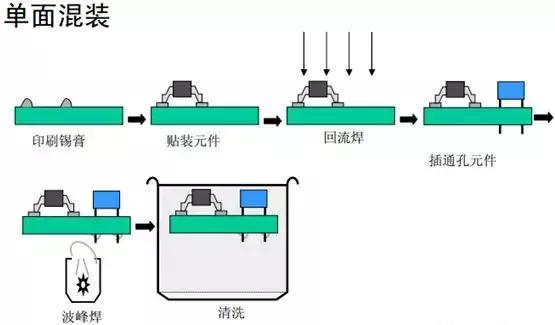
1.5.5 Double-sided mixed mount
The process flow is shown in the figure below
