What is the difference between PCB and PCBA?
There are many differences between PCB and PCBA
Definition and Structure different
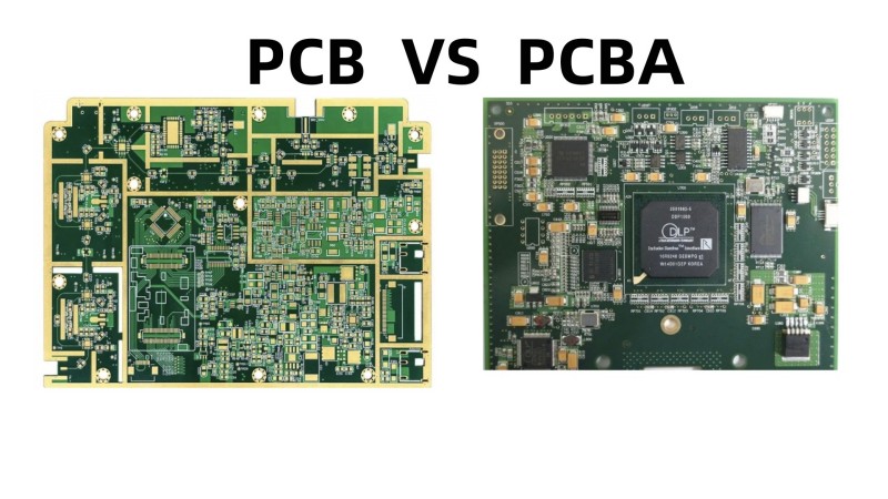
PCB is Printed Circuit Board which is a finished board on which printed circuits, printed components, or conductive patterns formed by the combination of both are made on an insulating substrate according to the predetermined design. Its basic structure is similar to a sandwich. For example, in a common two-layer board, the top and bottom are copper layers, and the middle is separated by non-conductive insulating materials like epoxy glass fiber. Multi-layer boards are formed by laminating multiple two-layer boards together.
PCBA is the abbreviation of Printed Circuit Board Assembly. It refers to the process of installing electronic components (such as chips, resistors, capacitors, etc.) onto a printed circuit board (PCB) through surface mount technology (SMT) or through-hole insertion (DIP) and other methods. After a series of technological processes like soldering and debugging, it finally forms a circuit board assembly with complete functions. For example, in the production of the mainboard of a mobile phone, there is a PCB first. Then, through the PCBA process, various tiny electronic components are installed on the PCB. After strict debugging, the mainboard can play functions such as signal processing and data storage normally. It is a key part for electronic devices to operate properly.
Function and Effect different
The functions and roles of PCB (Printed Circuit Board ) are mainly as follows:
- PCB provides mechanical support for the fixing and assembly of integrated circuits and other electronic components.
- PCB realizes the circuit and electrical connection or electrical insulation among electronic components, allowing the electric current to flow among the components along the pre-designed routes to perform functions such as doing work, amplification, and attenuation.
-PCB provides electrical characteristics like characteristic impedance.
-PCB offers solder mask patterns for automatic soldering and provides identification characters and patterns for component insertion, inspection, and maintenance.
The functions and roles of PCBA (Printed Circuit Board Assembly) are mainly as follows:
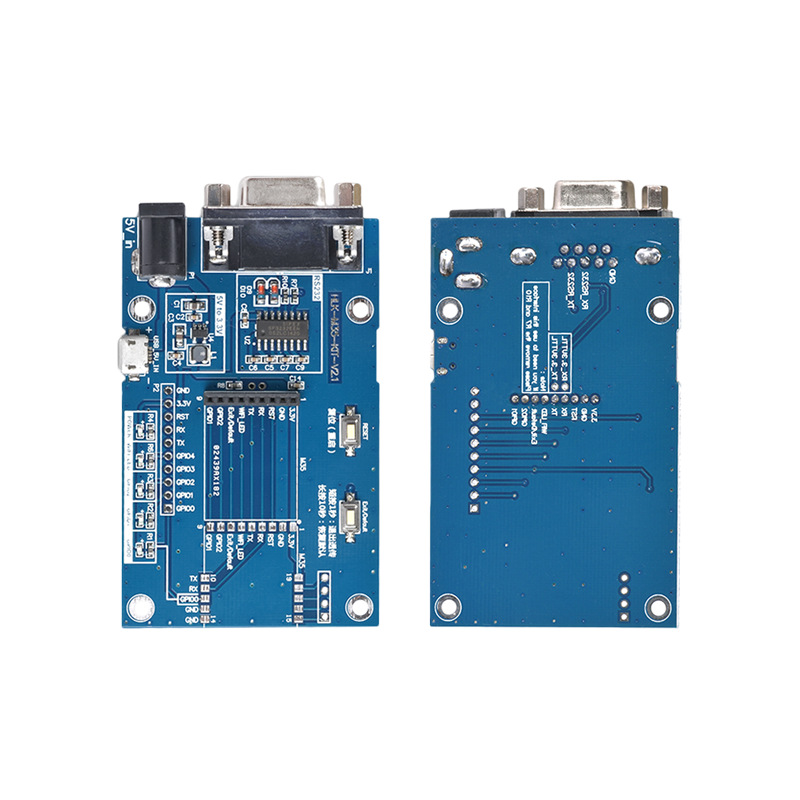
Realize Complete Electronic Functions
-PCBA can combine various electronic components together to form a complete circuit system. For example, in the PCBA of a computer motherboard, the interfaces of the CPU, memory, graphics card and other circuits are connected to each other through the circuits on the PCBA, thus realizing complex functions such as data processing, storage and display.
- It can precisely control the transmission of current, voltage and signals according to the specific product design requirements. For instance, in the PCBA for power management, by adjusting the component parameters in the circuit, it can stably output the voltage and current that meet the requirements of the equipment.
Signal Processing and Transmission
- PCBA can perform a variety of processing on the input signals, such as amplification, filtering, modulation and demodulation. Taking the radio frequency PCBA in mobile phones as an example, it can amplify and filter the received weak wireless signals, extract useful information, and at the same time modulate the signals to be sent so that they can be effectively transmitted through the antenna.
- PCBA ensures that signals are accurately and rapidly transmitted among various electronic components. Through reasonable wiring and signal integrity design, signal interference and attenuation are reduced. For example, the PCBA of high-speed digital circuits will adopt differential signal transmission and other methods to ensure signal quality.
Provide Physical Support and Electrical Connection
- PCBA provides a platform for the physical installation of electronic components and fixes the positions of the components. For example, on the PCBA of large servers, various heavy processors, heat sinks and other components installed on it rely on the PCBA to stabilize their positions.
- PCBA establishes reliable electrical connections so that all components can work together. The pins of each component are connected to the circuits on the PCBA through soldering and other methods to form a complete electrical network.
Element different
The main element of a PCB are as follows:
Base Material
It serves as the foundation of the PCB, providing mechanical support and electrical insulation. Common ones include FR-4 epoxy glass fiber cloth board and polyimide. FR-4 has high mechanical strength, good insulation properties, and a moderate price, so it is widely used. Polyimide is suitable for flexible and high-temperature environments.
Copper Layer
It forms conductive paths to connect electronic components and includes types such as single-sided boards, double-sided boards, and multi-layer boards. A single-sided board has a copper layer on only one side, with a low cost but a simple circuit design. A double-sided board has copper layers on both sides and can connect the circuits on both sides through vias, which is suitable for more complex circuits. A multi-layer board is formed by alternately laminating multiple copper layers and insulating materials, which can meet the requirements of complex electronic devices for space and high-speed signal transmission.
Pad
It is a metal hole used for soldering the pins of components. Its size, shape, and spacing need to be designed according to the size and layout requirements of the component pins to ensure the reliability and stability of soldering.
Via
It includes metal vias and non-metal vias. Metal vias are used to connect the pins of components between different layers to achieve electrical connections between layers. Non-metal vias are mainly used for mechanical fixation or as an auxiliary structure for conductive holes.
Mounting Hole
It is used to fix the circuit board onto the equipment housing or other supporting structures. Its position and size need to be determined according to the installation requirements of the equipment.
Conductor
Also known as circuit or trace, it is a copper film of the electrical network that connects the pins of components. Parameters such as its width, thickness, and spacing will affect the electrical properties of the circuit board, such as resistance, capacitance, and inductance.
Silk Screen Layer
It includes the top silk screen layer and the bottom silk screen layer, usually white, and is mainly used to place printed information, such as the outlines of components, labels, nominal values, model numbers, and various annotation characters, which facilitates component soldering and circuit inspection on the circuit board.
Mask Layer
It mainly includes the solder mask layer and the solder paste layer. The solder mask layer can prevent solder from flowing to places where it should not be soldered during soldering, avoiding problems such as short circuits. The solder paste layer is used to determine the application position of solder paste in the surface mount process.
Mechanical Layer
It is used to place instructive information about board manufacturing and assembly methods, such as the outline dimensions of the PCB, dimension marks, data information, via information, assembly instructions, etc.
Drill Layer
It includes drill holes (NC file layer), hole diameter diagrams, and position diagrams, which are respectively used to illustrate the size attributes of drill holes, show the size and position attributes of drill holes in graphics, and only mark the center point positions of drill holes.
The elements of PCBA mainly include the following parts:
Printed Circuit Board (PCB)
This is the fundamental part, providing physical support and electrical connection paths for the entire assembly. There are intricate copper foil circuits on it for conducting electric current, as well as various pads for connecting electronic components. For example, on the PCB of a computer motherboard, it is covered with circuits and numerous pads used for installing components such as the CPU and memory.
Electronic Components
- Active Components: Such as integrated circuit (IC) chips, which are the core parts of the entire PCBA and can perform complex functions like signal processing, data storage, and calculation. Taking the processor chip in a mobile phone as an example, it controls various functions of the mobile phone, including running applications and processing communication signals.
- Passive Components: They include resistors, capacitors, and inductors. Resistors are used to limit the magnitude of current. For instance, in the PCBA of an LED lamp, the resistor is used to control the current flowing through the LED to make its brightness appropriate. Capacitors are mainly used for storing electrical energy, filtering, etc. In the PCBA of a power supply circuit, capacitors can filter out the noise in the power supply. Inductors play a role in circuits related to electromagnetic induction. For example, they are used for energy conversion in some PCBA for wireless charging.
Welding Materials
The main material is solder, which is used to firmly connect the pins or terminals of electronic components to the pads on the PCB. In the Surface Mount Technology (SMT) process, solder paste is used, and the components are soldered onto the PCB through reflow soldering. In the Through-Hole Insertion (DIP) process, solid solder wire is adopted, and the welding is completed through wave soldering and other methods.
Other Auxiliary Parts
- Connectors: They are used to connect different circuit boards or external devices. For example, the USB ports and HDMI ports on a computer motherboard are convenient for plugging in and unplugging external devices, enabling data transmission and function expansion.
- Heat Sinks: Some PCBA components with higher power will be equipped with heat sinks. For example, the heat sink of a computer CPU is used to dissipate the heat generated by components during the working process, preventing the components from being damaged due to overheating and ensuring that the PCBA can work stably.
Processing different
The production process of PCB mainly includes the following steps:
PCB Design
According to the requirements of circuit functions and performance, professional design software is used to draw schematic diagrams, perform layout and routing, etc., determine the physical size, number of layers, graphics of each layer, and electrical connection relationships of the PCB, and generate Gerber files and other files required for manufacturing.
PCB Material Cutting
The original copper-clad laminate is cut into boards of appropriate sizes according to the design requirements. High-precision cutting equipment needs to be used to ensure dimensional accuracy and provide suitable blanks for subsequent processing.
PCB Inner Layer Circuit Fabrication
It includes multiple processes such as inner layer film lamination, exposure and development, inner layer etching, and film stripping. First, a photosensitive dry film is laminated on the surface of the inner layer copper plate. Then, the pattern on the negative film is transferred to the dry film through exposure. After that, the unexposed dry film is removed through development. Next, the exposed copper surface is etched away with an etching solution to form the inner layer circuit pattern. Finally, the film is stripped to obtain the inner layer circuit board.
PCB Browning Treatment
Through chemical treatment, a microscopic rough and organometallic layer is formed on the inner layer copper surface to enhance the adhesion between layers and prepare for the lamination process.
PCB Lamination
With the help of the adhesiveness of the PP sheet, the circuit boards of each layer, copper foil, bonding sheets, etc. are laminated according to the process requirements and pressed under high temperature and high pressure so that each layer is bonded into a whole to form a multi-layer board structure.
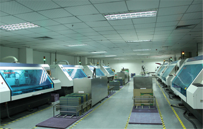
PCB Drilling
A high-precision drilling machine is used to drill through holes on the circuit board for electrical connection between different layers or for installing components. During drilling, it is necessary to ensure that the hole walls are smooth and free of burrs, and the hole diameter accuracy meets the requirements.
PCB Copper Plating in Holes
The PCB board after drilling is chemically treated so that a thin and uniform copper layer is deposited on the hole walls to realize the metallization of the holes and ensure electrical connection between layers.
PCB Panel Plating
The copper on the surface and in the holes of the PCB board just after copper plating in holes is thickened to prevent the thin copper in the holes from being oxidized or slightly etched away before pattern electroplating and exposing the substrate.
PCB Outer Layer Circuit Fabrication
It is similar to the inner layer circuit fabrication, including processes such as outer layer dry film lamination, exposure and development, outer layer pattern electroplating, and etching to form the outer layer circuit pattern and etch away the useless copper on the board surface.
PCB Solder Mask
A solder mask layer is applied on the board surface through screen printing or coating solder mask ink, and then exposed and developed to expose the pads and holes for soldering to prevent short circuits during soldering.
PCB Silk Screen Printing of Characters
Words, trademarks, component symbols, etc. are printed on the board surface by screen printing and then exposed to ultraviolet light for curing to facilitate the identification and assembly of the circuit board.
PCB Surface Treatment
To prevent the oxidation of the copper surface and improve solderability or electrical performance, the PCB board needs to be subjected to surface treatment. Common methods include HASL (Hot Air Solder Leveling), immersion gold, and OSP (Organic Solderability Preservative), etc.
PCB Shaping
A CNC shaping machine is used to cut the PCB board into the required external dimensions to ensure dimensional accuracy and edge quality.
PCB Electrical Testing
The actual working state of the board is simulated, and the board is powered on to check whether there are electrical performance problems such as open circuits and short circuits to ensure product quality.
PCB Final Inspection, Sampling Inspection, and Packaging
A comprehensive inspection is carried out on the appearance, size, hole diameter, board thickness, markings, etc. of the board. Qualified products that meet the requirements are packaged in bundles for storage and transportation.
The production process of PCBA mainly covers the following key steps:
Component Procurement and Inspection
- Firstly, according to the designed circuit schematic diagram and Bill of Materials (BOM), various electronic components such as chips, resistors, capacitors, and inductors are procured. During the procurement process, strict quality control is enforced, requiring suppliers to provide quality certificates to ensure that the parameters and specifications of the components meet the established design standards.
- After the components arrive, strict inspections are carried out. For example, an appearance inspection is conducted to check whether there is any damage or if the pins are bent. Professional testing equipment is also used to randomly test the electrical performance of some components, and non-conforming products are removed to lay a good foundation for subsequent assembly.
PCB Preparation
- Obtain the printed circuit boards (PCB) that have been manufactured from PCB manufacturers and check whether there are scratches on the appearance, whether the circuits are conductive, and whether the quality of the pads is qualified.
- According to the requirements of the production process, pre-treat the PCB by cleaning and baking it to remove dust, moisture, and other impurities that may exist on the surface, so as to avoid problems such as (solder joint insufficiency) and short circuits during the subsequent soldering and assembly process.
Solder Paste Printing
- Use specialized solder paste printing equipment to evenly print the solder paste onto the corresponding pads of the PCB. During this process, the printing parameters such as scraper pressure, printing speed, and demolding speed need to be precisely adjusted to ensure that the printing thickness, shape, and position of the solder paste are accurate, creating conditions for the accurate soldering of components.
Component Mounting (SMT)
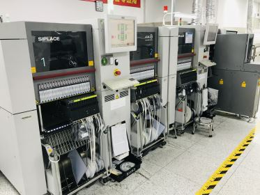
- Through automated pick-and-place machines, surface mount components (SMT) are accurately mounted onto the positions of the pads printed with solder paste on the PCB according to the preset program and layout. The pick-and-place machines have a high mounting speed and precision, and can complete the mounting of a large number of components in a short time while ensuring that the position deviation of each component is controlled within a very small range.
- After the mounting is completed, visual inspection is carried out. The optical inspection system is used to check whether the components are accurately mounted, whether there is any offset, and whether the solder paste is in good condition. Any problems found will be corrected in time or the defective products will be removed.
Reflow Soldering
- The PCB with mounted components enters the reflow soldering equipment and goes through multiple temperature zones such as preheating, heat preservation, reflow, and cooling. This causes the solder paste to melt under heat, thereby forming reliable solder joints between the component pins and the PCB pads and firmly soldering the components onto the PCB.
- During the reflow soldering process, the temperature, time of each temperature zone, and the speed of the conveyor belt need to be strictly controlled to ensure stable soldering quality and avoid soldering defects such as insufficient soldering and solder bridging.
Insertion (DIP) and Wave Soldering (if necessary)
- For some through-hole components that cannot be processed by the surface mount technology, they are inserted into the corresponding holes on the PCB manually or with the help of semi-automatic equipment.
- Subsequently, the wave soldering equipment is used to make the PCB pass through the molten solder wave so that the pins of the through-hole components are soldered to the PCB pads. Similarly, various parameters of the wave soldering, such as the solder temperature, wave height, and conveyor speed, need to be controlled to ensure the soldering effect.
Cleaning and Testing
- After soldering is completed, specialized cleaning solvents and equipment are used to clean the PCBA to remove impurities such as flux residues and solder slag left during the soldering process, preventing them from having an adverse impact on the performance and long-term stability of the PCBA.
- Then, comprehensive testing is carried out, including electrical performance testing, such as open circuit and short circuit detection, as well as functional testing, to ensure that the PCBA can normally achieve all the functions required by the design. Products that do not meet the requirements will be marked for repair or scrapped.
Burn-in Testing
- The PCBA that has passed the inspection is placed in burn-in testing equipment to simulate the state of long-term operation in the actual use environment. It is observed whether there will be performance degradation, failures, or other situations during the operation for a certain period of time, further verifying the reliability and stability of the product.
Finished Product Assembly and Packaging
- After the burn-in test confirms that there are no problems again, the PCBA will be assembled with other accessories (such as housings, display screens, buttons, etc., if applicable) to form a complete finished product.
- Finally, the finished PCBA is packaged. Appropriate packaging materials are selected, and protective measures against moisture, static electricity, and impact are taken. Corresponding identification labels are attached, indicating the product model, batch number, production date, and other information for easy storage, transportation, and subsequent quality traceability.
Appearance different
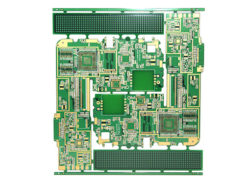
A PCB (Printed Circuit Board) is in a bare board state without any electronic components. Its appearance typically features the following: In terms of color, it is mostly green, but can also be blue, yellow, black, etc. The surface has a uniform paint film, free from marks, wrinkles, bubbles, etc., and the color difference and glossiness of the coating must meet the specified standards. Regarding the circuits, the circuit width, circuit thickness, and line spacing comply with the design requirements, with clear and regular lines and no defects such as short circuits or open circuits. The pads are smooth and flat on the surface, without oxidation or deformation issues.
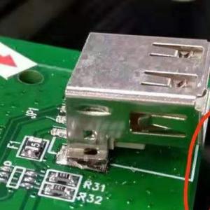
On the other hand, a PCBA (Printed Circuit Board Assembly) is a finished board after the printed circuit board has been assembled, with various electronic components such as chips, resistors, and capacitors soldered or mounted on it. Its appearance mainly includes the following aspects: The layout and installation of the components are carried out in accordance with the design requirements, arranged neatly and compactly, and positioned accurately without any deviation. The solder joints are firm, full, and smooth, without defects such as poor soldering, missing soldering, or solder bridging. In addition, there may be some markings and texts, such as the model, parameters, and polarity markings of the components, as well as printed labels for the product model, batch number, and production date. These markings are clear, accurate, and complete.
