Description
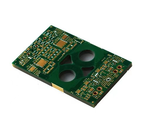
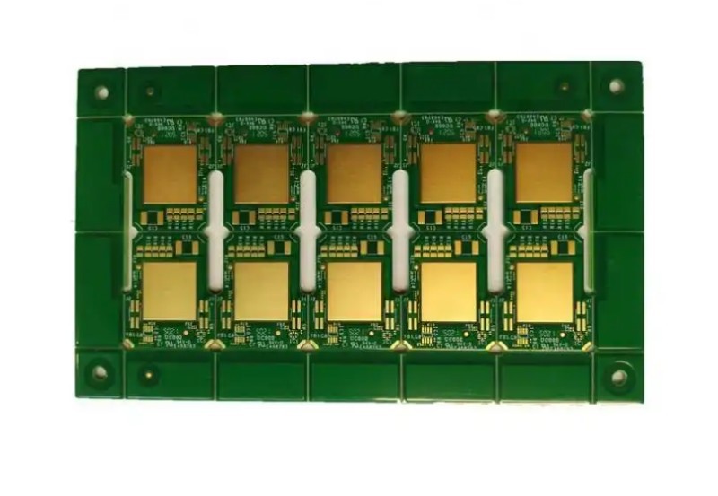
material is FR-4 with green soldermask,
surface treatment ENIG (immersion gold) ,
high TG 170, IPC class III,
1oz copper thick,
1.6mm board thick
min hole 0.3mm
min trace width/min distance 12mil
Product application: automobile power board
What is a heavy/thick copper PCB?
A heavy/thick copper PCB is a printed circuit board that has a copper layer with a thickness significantly greater than the standard thickness found in typical PCBs. The standard copper thickness in regular PCBs is usually around 1 oz (35 μm) per square foot. Heavy copper PCBs, on the other hand, can have copper thicknesses ranging from 3 oz (105 μm) up to 20 oz (700 μm) or even more per square foot.
These heavy/thick copper layers are used in applications where high current-carrying capacity, superior heat dissipation, or enhanced mechanical strength is required. They are commonly found in power electronics, automotive systems, industrial equipment, and other high-performance and demanding applications.
There are several types of heavy/thick copper PCBs, including:
1. Double-sided heavy/thick copper PCB: Copper is plated on both sides of the board to achieve a thick copper layer.
2. Multilayer heavy/thick copper PCB: Consisting of multiple layers with heavy copper plating on specific layers or throughout the board.
3. High current carrying heavy/thick copper PCB: Specifically designed to handle high electrical currents.
4. High thermal conductivity heavy/thick copper PCB: Useful in applications where efficient heat dissipation is crucial.
How thick is the copper layer in a heavy/thick copper PCB?
In a heavy/thick copper PCB, the copper layer thickness is typically considered to be 3 ounces or more per square foot. Commonly, it can range from 3 ounces to 20 ounces or even thicker in some specialized applications.
For reference, 1 ounce of copper is approximately equal to 1.4 mils (0.0356 mm) in thickness. So, a 3-ounce copper layer would be approximately 4.2 mils (0.107 mm) thick.
The applications of heavy/thick copper PCB in circuits mainly include the following aspects:
- High-power and high-frequency circuits: Heavy/thick copper PCB has low resistance and high thermal conductivity performance, which can withstand relatively large current and power, while reducing the loss and delay in signal transmission, and is suitable for high-power amplifiers, power modules, radio frequency circuits, etc.
- Devices with large current and high heat dissipation requirements: Some devices such as power supplies, motor drivers, electric vehicle charging piles, etc. need to handle large current and high heat dissipation. Heavy/thick copper PCB can provide better conductivity and heat dissipation performance to ensure the stability and reliability of the equipment.
- Industrial control and automation equipment: In the field of industrial control, heavy/thick copper PCB is often used in driving motors, control circuits and sensor interfaces, etc. Its reliability and anti-interference ability are crucial for stable operation in the industrial environment.
- Automotive electronics: Engine control units, braking systems, body electronics, etc. in automotive electronic systems all require PCBs with high reliability and high temperature resistance. Heavy/thick copper PCB can meet these requirements.
- Aerospace and military applications: In the aerospace and military fields, the requirements for the reliability and performance of PCBs are extremely high. Heavy/thick copper PCB is often used in key circuits such as flight control systems, radar systems, and navigation equipment.
- Renewable energy systems: Renewable energy equipment such as solar inverters and wind power generation control systems also often use heavy/thick copper PCB to cope with the requirements of high current and high power.
- Medical equipment: Some medical equipment such as X-ray machines and MRI have strict requirements on the performance and reliability of the PCB, and heavy/thick copper PCB can provide better electrical performance and anti-interference ability.
How to determine the cost difference between heavy/thick copper PCBs and normal PCBs?
To determine the cost difference between heavy/thick copper PCBs and normal PCBs, you need to consider the following factors:
1. Copper thickness: The main distinction is the thickness of the copper layer. Measure and compare the copper thickness in ounces per square foot for both types. The greater the difference, the more significant the cost disparity is likely to be.
2. Board complexity: Evaluate the design complexity of the PCB, including the number of layers, trace density, hole size and density, and any special features or requirements. More complex designs increase manufacturing costs.
3. Manufacturing process: Different manufacturing processes and techniques are used for heavy/thick copper and normal PCBs. Consider the plating methods, etching processes, and additional steps needed for heavy copper plating.
4. Quantity: The number of PCBs ordered can impact the unit cost. Larger quantities often result in lower per-unit costs due to economies of scale.
5. Supplier and location: The choice of the PCB manufacturer and their location can affect costs. Different suppliers may have different pricing structures and overheads.
6. Quality and reliability requirements: If higher quality and reliability standards are demanded for the PCBs, this can add to the cost.
To obtain an accurate cost comparison, it is best to request quotes from multiple PCB manufacturers, providing detailed specifications for both the heavy/thick copper and normal PCB designs. This will allow you to directly compare the prices and understand the specific factors contributing to the cost difference for your particular requirements.
Are heavy/thick copper PCBs more expensive than normal PCBs?
Yes, heavy copper PCBs are typically more expensive than normal PCBs.
The increased cost is mainly due to several factors. The manufacturing process for heavy copper PCBs is more complex and requires specialized equipment and techniques. Thicker copper plating often demands longer processing times and more advanced plating chemicals.
Also, the materials used for heavy copper PCBs may be of higher quality and cost. Moreover, the inspection and testing procedures to ensure the quality and performance of the thick copper layers add to the overall production costs.
However, in applications where the enhanced current-carrying capacity and heat dissipation provided by heavy copper are essential, the added cost is justified by the improved functionality and reliability of the PCB.
How much more expensive are heavy copper PCBs compared to normal PCBs?
The cost difference between heavy/thick copper PCBs and normal PCBs can vary significantly depending on a number of factors such as the thickness of the copper layer, the complexity of the board design, the quantity ordered, and the manufacturing facility.
Generally, heavy/thick copper PCBs can be 20% to 50% or even more expensive than normal PCBs. However, in some cases with very thick copper layers or complex requirements, the price increase could be even higher.
Are there any common methods for reducing the cost of heavy/thick copper PCBs?
There are several common methods for potentially reducing the cost of heavy/thick copper PCBs:
1. Optimize the copper layer thickness: Carefully assess the actual current-carrying and heat dissipation requirements to determine if the copper layer can be slightly thinner than the maximum specified without sacrificing performance. This fine-tuning can lead to cost savings.
2. Streamline the PCB design: Minimize the area of heavy/thick copper plating by optimizing the circuit layout. Reduce unnecessary copper coverage and simplify the design to the extent possible without compromising functionality.
3. Negotiate with suppliers: Work closely with PCB manufacturers and negotiate better prices based on volume orders or long-term partnerships.
4. Consider alternative materials: Explore alternative copper alloys or laminates that may offer similar performance at a lower cost.
5. Improve manufacturing yield: Ensure the design is manufacturable with high yield rates to minimize waste and rework, which can add to costs.
6. Batch production: Order larger quantities of the heavy/thick copper PCBs to take advantage of economies of scale and potentially obtain better unit prices.
However, it's important to note that while cost reduction is a goal, it should not compromise the quality and performance of the PCB for its intended application.
Are there any design guidelines or rules of thumb for minimizing the area of heavy/thick copper plating?
Yes, there are some design guidelines and rules of thumb for minimizing the area of heavy/thick copper plating in heavy/thick copper PCBs:

1. Route traces efficiently: Optimize the routing of traces to avoid unnecessary wide copper areas. Use narrower traces where possible without sacrificing current-carrying capacity.
2. Group components and current paths: Identify areas where high current is actually needed and concentrate the heavy/thick copper plating only in those specific regions.
3. Use thermal vias: Instead of having a large continuous copper area for heat dissipation, strategically place thermal vias to transfer heat more effectively and reduce the need for extensive copper plating.
4. Analyze current distribution: Conduct a detailed analysis of the current flow in the circuit to determine the exact areas that require heavy/thick copper and avoid over-plating elsewhere.
5. Consider power planes: If possible, use power planes with appropriate thickness rather than extensive heavy/thick copper plating throughout the board.
6. Follow manufacturing capabilities: Be aware of the manufacturing limitations and design within those parameters to avoid additional processing costs associated with complex or non-standard designs.
Remember, it's crucial to balance the minimization of copper area with maintaining the electrical and thermal performance requirements of the PCB.


