Description
What is PCB assembly?
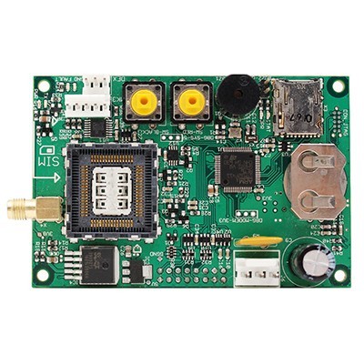
PCB assembly refers to the process of mounting and soldering electronic components onto a printed circuit board (PCB) to create a functional electronic circuit.
This involves various steps such as placing components accurately on the PCB pads, applying solder to form electrical connections, and conducting quality checks to ensure the assembled PCB meets the required specifications and functions properly. PCB assembly is a crucial part of the electronics manufacturing process, enabling the creation of complex and reliable electronic devices and systems.

PCB Assembly Factory Manufacturing Process
PCB (Printed Circuit Board) assembly is the key manufacturing process of installing and connecting electronic components onto a PCB to create a fully functional electronic product. The following is a detailed description of the common manufacturing process in a PCB assembly factory:
1. PCB Design and Fabrication
Before starting the assembly, the PCB design is the first step. Engineers use professional electronic design automation (EDA) software to plan the circuit layout, determine the positions of components and the connection methods. Once the design is completed, manufacturing files for the PCB, including schematics, wiring diagrams and layer stack-up structures, are generated.
PCB manufacturing typically employs lithography and etching techniques. The base material of the substrate (such as glass fiber-reinforced epoxy resin) is cut and drilled to form holes for component installation and pathways for circuit connections. Then, conductive layers, such as copper, are added to the board through chemical deposition or electroplating processes. Next, using photoresist and exposure equipment, the circuit pattern is transferred onto the copper layer, and the unwanted copper is removed by etching, leaving behind precise circuit traces.
2. PCB Assembly Factory purchase component and Preparation
According to the design requirements of the PCB, the necessary electronic components are purchased. This includes integrated circuits (ICs), resistors, capacitors, inductors, connectors, etc. The procurement of components requires ensuring the accuracy of their quality, specifications and quantity.
After the components arrive at the factory, quality inspections are conducted to check for any damage, oxidation of pins or other defects. For surface mount devices (SMDs), they are usually wound on reels for automatic pick-and-place machines to pick up; for through-hole devices (THDs), they need to be classified and sorted.
3. PCB assembly factory Solder Paste Printing
For the assembly of surface mount components, solder paste printing is performed first. Solder paste is a paste composed of tiny solder balls and flux. Using a solder paste printer, a stencil (with openings corresponding to the component pads on the PCB) is placed on the PCB, and then the solder paste is evenly extruded through the openings of the stencil using a squeegee and deposited on the solder pads of the PCB.
The quality of solder paste printing is crucial for subsequent component placement and soldering. After printing, it is necessary to check the thickness, uniformity of the solder paste and the presence of any missing or short-circuit issues.
4. Component Placement
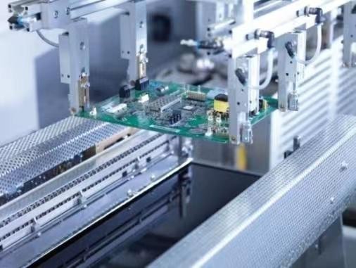
After the solder paste printing, the PCB is sent to a pick-and-place machine for component placement. Modern pick-and-place machines are usually highly automated equipment that can quickly and precisely pick up components and place them on the corresponding solder pads on the PCB.
The pick-and-place machine in operates in PCB assembly factory based on pre-programmed component position information and placement sequence. For small and high-precision components, high-speed pick-and-place machines are usually used; while for large and special-shaped components, multi-functional pick-and-place machines or manual assistance may be required.
During the component placement process, the accuracy and precision of the placement need to be monitored in real-time to ensure that the orientation, position and spacing of the components meet the design requirements.
5. Reflow Soldering in PCB assembly factory

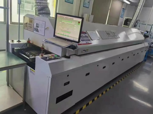
The PCB with components placed is sent into a reflow soldering oven for soldering. The reflow soldering oven has different heating zones inside and can precisely control the temperature profile.
During the heating process, the flux in the solder paste first volatilizes to remove oxides on the surfaces of the PCB and component pins. As the temperature rises, the solder paste melts to form liquid solder, which tightly connects the component pins to the PCB pads. When the temperature cools down, the solder solidifies to form reliable solder joints.
The temperature profile of reflow soldering needs to be optimized based on the type of solder paste, the number of PCB layers and the characteristics of the components to ensure soldering quality and avoid damage to the components due to thermal stress.
6. Through-Hole Component Installation PCB assembly factory
For through-hole components, they are installed by manual or wave soldering after reflow soldering is completed. In manual installation, workers insert the component pins into the through holes of the PCB and perform soldering using manual soldering tools.
Wave soldering involves passing the PCB through a flowing liquid solder wave to allow the pins to contact the solder and complete the soldering. Before wave soldering, the PCB needs to be pretreated, such as pre-coating with flux.
7. Soldering Inspection
After soldering in PCB assembly factory, the soldering quality is inspected. Common inspection methods include visual inspection, automatic optical inspection (AOI) and X-ray inspection.
Visual inspection is used to detect obvious soldering defects such as cold solder joints, short circuits and pin offsets. The AOI system can automatically detect more minor soldering defects through optical imaging and image analysis technology. X-ray inspection is used to examine the solder joint conditions inside packages such as BGA (Ball Grid Array).
For any soldering defects found, rework and repair are necessary to ensure the reliability of the PCB.
8. Cleaning in PCB assembly factory
To remove the flux, solder paste and other contaminants remaining from the soldering process, the PCB may need to be cleaned. Cleaning methods include solvent cleaning, water cleaning and no-clean technologies, depending on the application and requirements of the PCB.
9. Testing and Debugging
The PCB after assembly and soldering needs to undergo functional testing and debugging to ensure it meets the design specifications and performance requirements. Tests may include circuit connectivity testing, electrical parameter measurement and functional module testing.
For complex PCB systems, system-level testing and integration testing may also be required. During the testing process, any problems found require fault diagnosis and repair.
10. Three-Protection Treatment (Optional) in PCB assembly factory
In some applications, to improve the protection performance of the PCB, a three-protection treatment may be performed, that is, coating a layer of protective coating for waterproofing, moisture-proofing and dust-proofing.
11. Packaging and Shipping
After passing the tests, the PCB is packaged to protect it from damage during transportation and storage. The packaging method is usually determined based on the size and quantity of the PCB and customer requirements.
Finally, the PCB is shipped to the customer for assembly and production of electronic products.
In conclusion, the manufacturing process of a PCB assembly factory is a complex and precise process involving strict control and quality inspection in multiple links to ensure the production of high-quality, high-performance and reliable PCB products to meet the needs of various electronic devices. The optimization and improvement of each step helps to improve production efficiency, reduce costs and enhance product quality, thereby maintaining an advantage in the highly competitive electronic manufacturing industry.
The following are some common types of PCB soldering in assembly factory:
1. Reflow Soldering in PCB assembly factory: This is a commonly used soldering method in Surface Mount Technology (SMT). Solder paste is first printed on the solder pads of the PCB, and then surface mount components are placed at the corresponding positions. Heating is applied to melt the solder paste to complete the soldering.
2. Wave Soldering in PCB assembly factory: It is mainly used for soldering between through-hole components and the PCB. The PCB passes through a molten solder wave, allowing the component leads to complete soldering with the through-hole solder pads on the PCB.
3. Manual Soldering: In some cases, such as repair, prototyping, or small-scale production, soldering is performed manually using an electric soldering iron and solder wire.
4. Selective Wave Soldering in PCB assembly factory: Wave soldering is carried out for specific solder joints rather than the entire PCB.

5. Laser Soldering: A laser is used as the heat source to melt the solder for soldering.
These soldering methods have their own characteristics and application scenarios. In the PCB manufacturing process, the appropriate soldering method is usually selected based on production requirements and the design of the PCB.
What are the advantages of selective wave soldering in PCB assembly factory?
Selective wave soldering has the following advantages:
1. Precise soldering: It is capable of precisely soldering specific solder joints, reducing the thermal impact on areas that do not require soldering in PCB assembly factory, thereby minimizing potential damage to surrounding components and the PCB itself.
2. Reduced bridging and short circuits: Since it is selective soldering, it can effectively avoid bridging and short circuit problems caused by the flow of solder between adjacent solder joints.
3. Adaptability to complex circuit boards of PCB assembly factory: For complex PCB boards with high density and diverse component layouts, it can flexibly handle solder joints of different types and locations.
4. Reduced use of flux and solder: Flux and solder are applied only at the required soldering areas in PCB assembly factory , saving material costs and reducing the subsequent cleaning workload.
5. Reduced thermal stress: Local heating reduces the thermal stress endured by the entire PCB board, helping to improve the reliability and service life of the PCB and components.
6. Increased production efficiency: Compared to traditional wave soldering, its setup and programming are relatively simple, and it can quickly switch between different product soldering programs, enhancing the flexibility and production efficiency of the production line in PCB assembly factory.
7. Improved soldering quality: Precise temperature control and soldering process parameter settings contribute to obtaining more uniform and reliable solder joint quality.
Regarding whether a PCB assembly factory can meet the needs of both small-batch and large-batch PCB assembly, it depends on the scale, equipment, staffing, and production management capabilities of the factory.
Large-scale PCB assembly factories typically have more advanced automated equipment and complete production lines, and they can handle orders of different scales by optimizing the production process and resource allocation. They may have sufficient inventory and supply chain management capabilities to ensure a stable supply of raw materials for large-scale production and flexibly adjust the production plan to reduce waste during small-batch production.
Some smaller-scale PCB assembly factories may focus more on specific types or scales of orders, but through effective cooperation and resource integration, they may also be able to meet diverse needs.
In addition, the factory's quality management system and process level also play a key role in whether it can successfully handle orders of different scales. Factories with strict quality control and high-precision processes can ensure the consistency of quality and performance of PCB assembly, whether in small-batch or large-batch production.
In conclusion, to determine whether a PCB assembly factory can meet the needs of both small-batch and large-batch PCB assembly, it is necessary to comprehensively consider its various capabilities and resources. KEY TECH is a large-scale PCB assembly factory, It is a good choice for PCB assembly.


