FR-4 PCB Manufacturing process-Etching
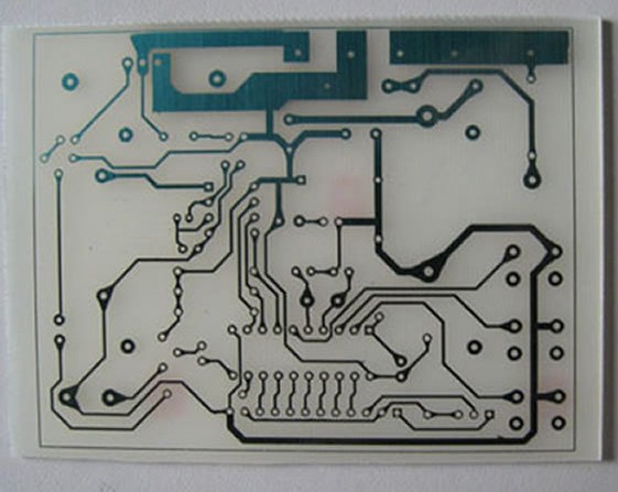
The FR-4 PCB manufacturing etching process in the fabrication of PCB (Printed Circuit Board) is a crucial step to precisely form the circuit pattern by selectively removing the unwanted copper foil.The FR-4 PCB manufacturing etching process is mainly divided into two main types: chemical etching and electrolytic etching.
Chemical etching is a commonly used method. At the beginning of this process, a layer of resist, usually photoresist or dry film, needs to be carefully coated on the surface of the copper-clad laminate. Through photolithography or other advanced exposure techniques, the resist in the parts of the circuit pattern that need to be retained is cured. The unexposed resist parts are then removed in the subsequent development process, exposing the underlying copper foil.
After completing the above preparations, the copper-clad laminate is carefully placed into the etching solution. Common FR-4 PCB manufacturing etching solutions include chemical solutions such as ferric chloride and cupric chloride. The chemical substances in these etching solutions undergo a series of complex and precise chemical reactions with the exposed copper foil, gradually and selectively dissolving the unwanted copper foil. During the entire etching process, several key factors need to be strictly and precisely controlled. The concentration of the etching solution is an important parameter. A too high concentration may lead to an overly fast etching rate, making it difficult to precisely control the depth and shape of the etching and may even cause damage to the copper foil that needs to be retained; a too low concentration will slow down the etching rate and affect production efficiency. Temperature also plays a crucial role. An increase in temperature usually accelerates the etching reaction rate, but an excessively high temperature may lead to a decrease in the stability of the etching solution and affect the consistency of the etching effect. In addition, the control of the etching time must be precise. If the etching time is too short, the unwanted copper foil cannot be completely removed; if the etching time is too long, over-etching may occur, damaging the integrity and precision of the circuit pattern. To ensure the full contact between the etching solution and the copper foil and achieve uniform etching, the stirring speed of the solution also needs to be reasonably set.

FR-4 PCB manufacturing electrolytic etching achieves the purpose of etching based on the principle of electrolysis. In the electrolytic etching process, the copper-clad laminate is placed as the anode in an etching tank containing a specific electrolyte. When direct current passes through, the copper on the anode undergoes an oxidation reaction and gradually dissolves into the solution, thereby achieving the etching effect. Compared with chemical etching, electrolytic etching has unique advantages in some specific cases. For example, for some complex shapes or circuit patterns with high precision requirements, electrolytic etching can provide more precise control and more uniform etching effect.
After the entire FR-4 PCB manufacturing etching process is completed, the remaining resist needs to be removed. This is usually achieved by cleaning with specially formulated solvents or alkaline solutions. If the resist is not completely removed, it may adversely affect the subsequent PCB fabrication processes, such as affecting the coating quality of the solder mask or causing instability in electrical performance.
During the implementation of the entire FR-4 PCB manufacturing etching process, the control of the following factors is crucial:
Firstly, the selection and ratio of the etching solution require careful consideration and experimental verification. Different etching solutions have distinct etching rates and etching effects. For example, ferric chloride etching solution has a relatively low cost but a relatively slow etching rate, and the side etching problem after etching may be more prominent; cupric chloride etching solution usually has a faster etching rate and better etching precision but a relatively high cost. Therefore, in actual production, the most suitable etching solution needs to be comprehensively selected based on specific requirements of the PCB, such as line precision, production efficiency, and cost budget, and the etching performance is optimized through precise ratio adjustment.
Secondly, the performance of the FR-4 PCB manufacturing etching equipment and the precise control of process parameters directly determine the quality of the etching. Advanced etching equipment can provide more stable temperature control, more uniform solution stirring, and more precise control of the etching time. At the same time, process parameters such as temperature, etching time, and solution stirring speed need to be repeatedly optimized and adjusted based on the characteristics of the etching solution, the design requirements of the PCB, and the performance of the equipment. Through real-time monitoring and feedback systems, deviations in the etching process are detected and corrected in a timely manner to ensure that each batch of PCBs achieves highly consistent etching quality.
In addition, the quality of the resist and the coating effect have a non-negligible impact on the successful implementation of the etching process. High-quality resist should have good adhesion, precise resolution, and excellent chemical corrosion resistance. During the coating process, it is necessary to ensure that the resist evenly covers the surface of the copper-clad laminate without bubbles, voids, or uneven thickness problems. The coating thickness also needs to be strictly controlled according to the requirements of the etching precision. A too thick coating may lead to a decrease in resolution, while a too thin coating cannot effectively resist the erosion of the etching solution.
In conclusion, the FR-4 PCB manufacturing etching process is a complex and crucial link in PCB fabrication, requiring a high degree of precise control and rich experience accumulation. Only by achieving excellence in each link can it be ensured that the final produced PCB has a high-quality circuit pattern and meets the strict requirements of modern electronic devices for high performance and high reliability.


