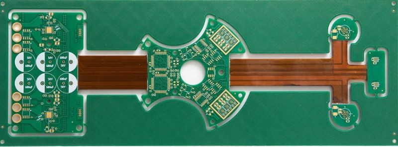
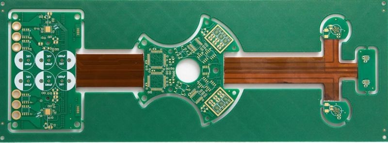
Description
Rigid-flex PCB design guidelines
1. Rigid-flex PCB design guidelines involve materials selection: Choosing appropriate base materials for the rigid and flexible sections, considering factors such as dielectric constant, dissipation factor, and thermal stability.
2. Rigid-flex PCB design guidelines involve layer stack-up: Defining the layer configuration to meet electrical performance, signal integrity, and mechanical requirements.
3. Rigid-flex PCB design guidelines involve flexibility considerations: Ensuring that the flexible portion can withstand the expected bending cycles without damage to the traces or components.
4. Rigid-flex PCB design guidelines involve trace routing: Planning the routing of traces to minimize crosstalk, impedance mismatches, and signal degradation.
5. Rigid-flex PCB design guidelines involve via design: Designing vias to provide reliable connections between layers and to avoid stress concentrations.
6. Rigid-flex PCB design guidelines involve component placement: Positioning components to optimize the board's performance and to minimize mechanical stress on the flexible areas.
7. Rigid-flex PCB design guidelines involve stiffener placement: Incorporating stiffeners in the right locations to provide support and prevent excessive flexing.
8. Rigid-flex PCB design guidelines involve design for manufacturability: Considering the capabilities and limitations of the manufacturing process to ensure high yield and quality.
9. Rigid-flex PCB design guidelines involve thermal management: Addressing heat dissipation to prevent overheating of components and to maintain reliable operation.
10. Rigid-flex PCB design guidelines involve testing and validation: Planning for effective testing methods to verify the functionality and performance of the rigid-flex PCB.

How to ensure signal integrity in rigid-flex PCB design?
To ensure signal integrity in rigid-flex PCB design, consider the following steps:
1. Accurate impedance control of rigid-flex PCB : Calculate and maintain the desired impedance for signal traces throughout the rigid and flex sections. This involves precise control of trace width, thickness, and dielectric properties.
2. Minimize rigid-flex PCB trace discontinuities: Reduce vias, bends, and transitions that can cause impedance variations and signal reflections. Use smooth curves and gradual transitions when possible.
3. Ground and power plane design of rigid-flex PCB: Implement proper ground and power planes to provide stable reference voltages and minimize noise coupling.
4. Controlled rigid-flex PCB impedance routing: Route high-speed signals on layers with controlled impedance and keep them away from noise sources.
5. Termination techniques of rigid-flex PCB: Use appropriate termination methods such as series termination, parallel termination, or AC coupling to minimize signal reflections.
6. Rigid-flex PCB shielding: Consider using shielding layers or shields around sensitive signal traces to protect them from external electromagnetic interference (EMI).
7. Rigid-flex PCB simulation and analysis: Perform pre-layout signal integrity simulations to predict and address potential issues before manufacturing.
8. rigid-flex PCB component placement: Position components to minimize signal path lengths and crosstalk. Keep high-speed components close to each other and away from noise-generating components.
9. Controlled dielectric materials of rigid-flex PCB: Select dielectric materials with consistent and low-loss characteristics to reduce signal attenuation.
10. Reduced stubs of rigid-flex PCB: Minimize the length of unused trace stubs, as they can cause signal reflections.
11. Decoupling capacitors of rigid-flex PCB: Place decoupling capacitors strategically to provide local charge reservoirs and stabilize power supply voltages.
By carefully addressing these aspects during the design process, you can significantly enhance signal integrity in rigid-flex PCB designs.

What are the common signal integrity problems in rigid-flex PCB design and how to solve them?
Common signal integrity problems in rigid-flex PCB design and their solutions are as follows:
Signal Reflections:
- Rigid-flex PCB design signal reflections problem: Signals bounce back and forth at impedance discontinuities, causing signal distortion and timing errors.
- Solution: Control impedance throughout the PCB by accurately designing trace widths, thicknesses, and dielectric properties. Use proper termination strategies like series or parallel termination.
Crosstalk:
- Rigid-flex PCB design crosstalk problem: Signals on adjacent traces interfere with each other, causing noise and signal degradation.
- Solution: Increase the separation between traces, use shielding or guard traces, and route sensitive signals away from noisy ones.
Signal Attenuation:
- Rigid-flex PCB design signal attenuation problem: Signals lose strength over the length of the traces, especially at high frequencies.
- Solution: Choose materials with low dielectric loss tangent, optimize trace geometries, and limit the length of high-frequency signal paths.
Delay and Skew:
- Rigid-flex PCB design delay and skew problem: Different signal paths have varying propagation delays, causing timing skew and synchronization issues.
- Solution: Equalize trace lengths for critical signals and use controlled impedance routing.
Power Supply Noise:
- Rigid-flex PCB design power supply noise problem: Fluctuations in the power supply voltage can affect signal quality.
- Solution: Place sufficient decoupling capacitors close to power-hungry components and design a low-impedance power distribution network.
Ground Bounce:
- Rigid-flex PCB design ground bounce problem: Sudden changes in current through the ground plane cause voltage fluctuations.
- Solution: Ensure a solid and continuous ground plane with low impedance and minimize the inductance in ground connections.
EMI/RFI (Electromagnetic Interference/Radio Frequency Interference):
- Rigid-flex PCB design EMI/RFI problem: The PCB can emit or be susceptible to external electromagnetic fields.
- Solution: Use proper shielding, ground planes, and filtering components.
Via Effects:
- Rigid-flex PCB design via effects problem: Vias can introduce impedance discontinuities and signal reflections.
- Solution: Optimize via size, stub length, and placement.
To solve these problems effectively, it's essential to perform signal integrity simulations during the design phase and make necessary adjustments before manufacturing.


