Description
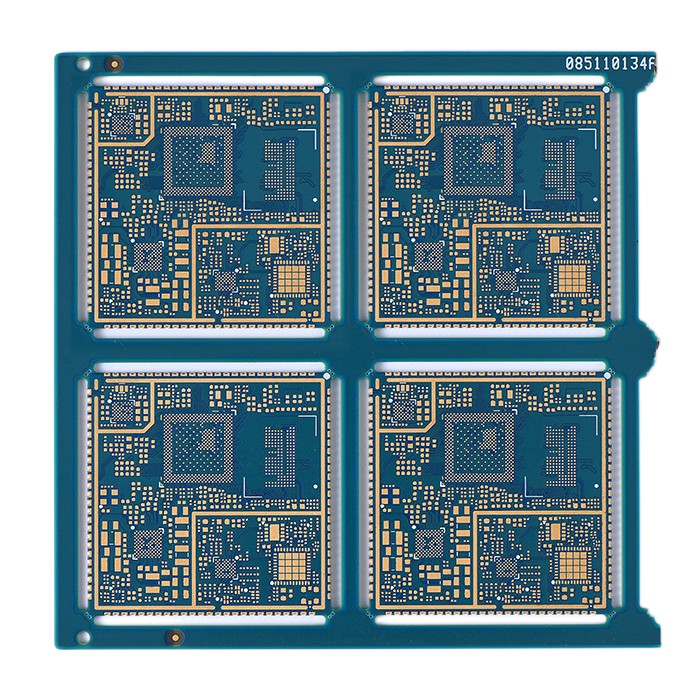
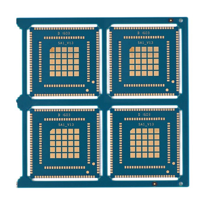
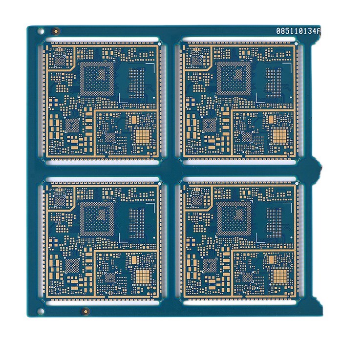
ENEPIG PCB is rigid, material is FR-4 with blue soldermask, surface treatment ENEPIG , edge plated high TG 170, IPC class III,1oz copper thick, 1.6mm board thick

In the production process of ENEPIG PCB, the main purposes of electroless nickel plating and electroless palladium plating are as follows. The main purpose of electroless nickel plating is to improve the solderability and corrosion resistance of the PCB. The nickel layer can act as a barrier layer between the copper layer and the gold layer to prevent the mutual diffusion of gold and copper, thereby affecting the solderability and service life of the PCB. In addition, the nickel layer can also improve the mechanical strength of the gold layer. The main purpose of electroless palladium plating is to improve the conductivity and oxidation resistance of the PCB. The palladium layer can act as a barrier layer to prevent the problem of copper migrating to the gold layer and causing poor solderability. At the same time, the electroless palladium plating layer will be completely dissolved in the solder, and there will be no appearance of a high-phosphorus layer at the alloy interface. When the electroless palladium is dissolved, a new electroless nickel layer will be exposed to form a good nickel-tin alloy.


