In the manufacturing process of PCB-lamination
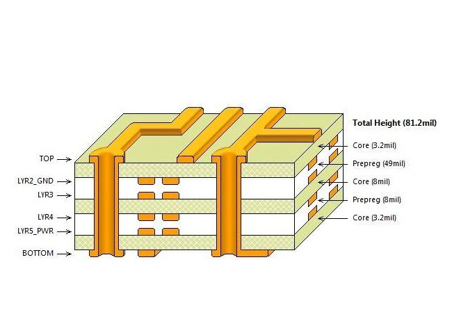
In the manufacturing process of PCB (Printed Circuit Board), the lamination step holds a crucial position. Its main role is to fuse multiple layers of different materials closely and stably together to construct a multilayer PCB structure. The following is a detailed and in-depth elaboration of this complex and key lamination process.Firstly, before the PCB manufactuering lamination process begins, thorough material preparation is indispensable. This stage is like the material preparation before building construction, which needs to be precise and error-free. The inner core layer, as the core component of the PCB, usually has undergone a series of pretreatment processes such as circuit fabrication, etching, and others, and its surface has formed fine and complex circuit patterns. The prepreg sheet, also known as the PP sheet, is a key material that plays a bonding role in the lamination process and has certain viscosity and fluidity. The outer copper foil, on the other hand, shoulders the important mission of forming the outer conductive layer of the PCB, providing the basis for the conduction of the circuit.
After the PCB manufacturing lamination materials are ready, the next step is the meticulous layering process. This is like building a skyscraper carefully, where the position and alignment accuracy of each layer are of utmost importance. According to the pre-designed layering structure, the inner core layer, the prepreg sheet, and the outer copper foil need to be precisely stacked in sequence. To achieve accurate alignment between each layer, positioning holes and specialized alignment tools are usually employed. These positioning holes and tools are like precise scales, ensuring that the positional deviation of each layer in both horizontal and vertical directions is controlled within a very small range. Even the slightest deviation may lead to incorrect circuit connections, thereby affecting the overall performance and functionality of the PCB.

After the PCB manufacturing process layering is completed, the pre-pressing step unfolds. This step is like a warm-up and preparation for the subsequent formal lamination. The entire layering structure is carefully placed in the press, and a certain pressure and temperature are applied. The main purpose of pre-pressing is to initially make each layer of material adhere to each other and expel as much air and excess resin trapped between the layers as possible. The presence of air may form bubbles during the subsequent high-temperature and high-pressure lamination process, and excessive uncured resin may lead to uneven resin flow, thereby increasing the risk of defects such as delamination. Through pre-pressing, the occurrence probability of these potential problems can be significantly reduced, laying a solid foundation for the subsequent high-quality lamination.
Next comes the core stage of the PCB manufacturing entire lamination process - high-temperature and high-pressure lamination. This stage is like a precise fusion experiment under high temperature and high pressure. Under the strict conditions where the temperature is usually set between 150 - 200°C and the pressure is usually maintained between 20 - 40 psi, the resin in the prepreg sheet undergoes profound physical and chemical changes. The high temperature significantly enhances the fluidity of the resin, enabling it to fully fill the tiny gaps between each layer and ensuring a tight bond. At the same time, the high pressure prompts the resin to distribute evenly during the flow process, avoiding local accumulation or vacancies. Under such extreme conditions, the resin undergoes a curing reaction, tightly bonding the inner core layer and the outer copper foil together, gradually forming a strong and stable multilayer structure. This multilayer structure is not only physically closely combined but also achieves good conduction and signal transmission between each layer in terms of electrical performance.
When the PCB manufacturing high-temperature and high-pressure lamination process ends, the cooling step becomes a crucial step to stabilize the structure and performance of the PCB. Just like hot steel becomes tough after quenching, after undergoing the high-temperature and high-pressure ordeal, the PCB needs to be cooled to fully cure the resin, thereby fixing the positions and structures of each layer. During the cooling process, the rate of temperature drop needs to be precisely controlled. Excessively rapid cooling may cause the generation of internal stress, affecting the flatness and reliability of the PCB; overly slow cooling may extend the production cycle and reduce production efficiency. Therefore, a scientifically and reasonably cooling strategy is crucial for ensuring the final quality and performance of the PCB.
The PCB manufacturing process after lamination is not yet complete and requires a series of fine subsequent processing steps to further improve its performance and meet the design requirements. Firstly, any excess or overflowing prepreg sheet that may have occurred during the lamination process needs to be removed. If these excess parts are not processed, they may affect the appearance size and subsequent installation and use of the PCB. Next, the surface of the PCB is polished to remove any possible tiny protrusions or unevenness, ensuring the flatness and smoothness of the surface and providing a good foundation for the subsequent circuit fabrication and component installation. In addition, according to the design requirements, drilling operations need to be performed. These drillings will be used for installing the pins of electronic components or achieving electrical connections between different layers. The accuracy and quality of the drilling directly relate to the assembly effect and electrical performance of the PCB.
Throughout the entire PCB manufacturing lamination process, each step has a profound impact on the final quality and performance of the PCB. The precision and stability of the lamination equipment are key factors in ensuring uniform pressure and temperature distribution and tight adhesion of each layer of material. A high-precision press can provide accurate and consistent pressure, ensuring a uniform effect throughout the lamination area. At the same time, a stable temperature control system can precisely control the heating and cooling processes, avoiding adverse effects of temperature fluctuations on resin curing and material performance.
The quality of the materials is equally important. High-quality inner core layers should have good flatness, uniform thickness, and consistent electrical properties. The resin content, fluidity, and curing characteristics of the prepreg sheet all need to meet strict standards to ensure the bonding effect and electrical performance during the lamination process. The thickness, purity, and surface roughness of the outer copper foil will also directly affect the conductive performance and reliability of the PCB.
In addition, the control of PCB manufacturing lamination parameters is the core point in the lamination process. The precise setting and strict monitoring of parameters such as pressure, temperature, and time are crucial for achieving high-quality lamination. Different types and thicknesses of PCBs may require different combinations of process parameters, which require experienced process engineers to optimize and adjust based on the actual situation. Simultaneously, the control of environmental conditions during the lamination process, such as cleanliness and humidity, can also reduce the potential interference of external factors on the lamination quality.
In conclusion, the lamination process in the PCB manufacturing process is a highly complex, precise, and key step. It requires strict material selection, precise equipment control, optimized process parameters, and fine subsequent processing. Only by strictly controlling and meticulously operating each step can high-quality and reliable multilayer PCBs be produced to meet the strict requirements of modern electronic devices for high-performance and high-density circuit boards.


